Semiconductor structure and forming method of semiconductor structure
A technology of semiconductor and gate structure, which is applied in the field of semiconductor structure and the formation of semiconductor structure, which can solve the problems that the performance and reliability of semiconductor devices need to be improved, and achieve the effect of improving performance and reliability
- Summary
- Abstract
- Description
- Claims
- Application Information
AI Technical Summary
Problems solved by technology
Method used
Image

Examples
Embodiment Construction
[0033] As mentioned in the background, the performance and reliability of semiconductor structures still needs to be improved. Now analyze and illustrate in conjunction with specific embodiment.
[0034] It should be noted that the "surface" in this specification is used to describe the relative positional relationship in space, and is not limited to direct contact.
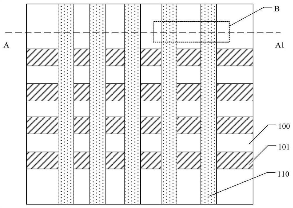
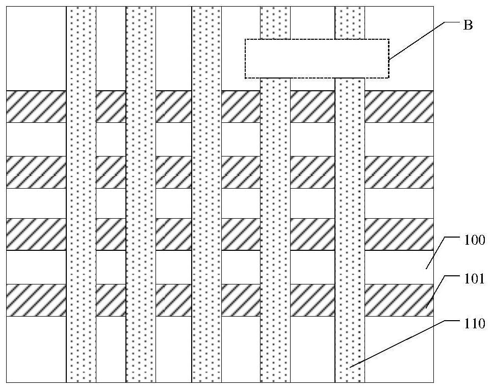
[0035] Figure 1 to Figure 3 It is a structural schematic diagram of each step in the formation process of a semiconductor structure.
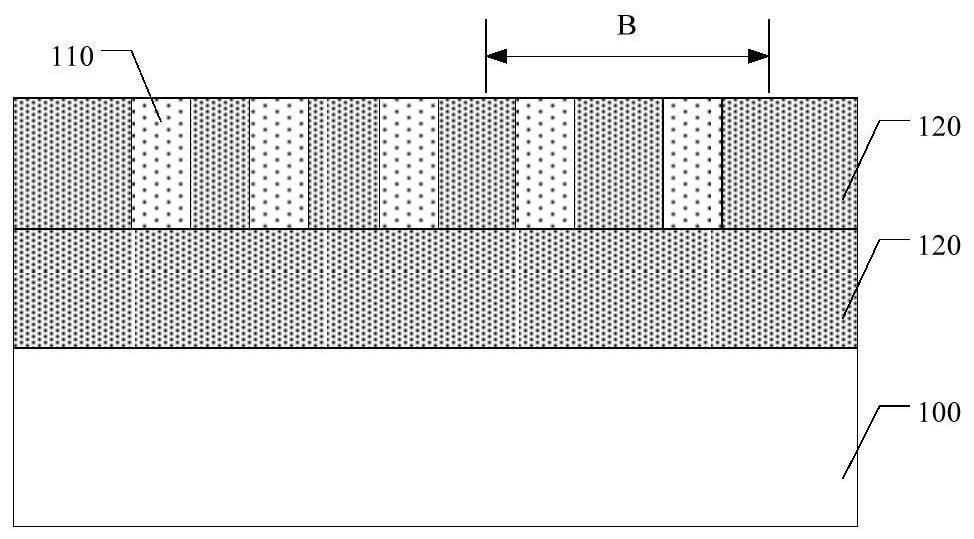
[0036] Please refer to Figure 1 to Figure 2 , figure 1 is a schematic top view of a semiconductor structure, figure 2 yes figure 1The schematic cross-sectional structure along the direction A-A1 in the figure provides a substrate 100, the substrate 100 includes an isolation region B, the substrate 100 has several fin structures 101 separated from each other; a first dielectric structure 120 and a plurality of fin structures 101 are formed; across the gate structure 110 o...
PUM
 Abstract
Description
Claims
Application Information