Three-dimensional reconfigurable broadband wide-angular-domain wave-absorbing material based on Miura origami

A technology of wave absorbing material and origami structure, applied in electrical components, antennas and other directions, can solve the problems of small thickness and poor performance of wave absorbing materials, and achieve the effects of low processing cost, efficient absorption and simple preparation

Pending Publication Date: 2022-01-25
AIR FORCE UNIV PLA
View PDF2 Cites 4 Cited by
  • Summary
  • Abstract
  • Description
  • Claims
  • Application Information

AI Technical Summary

Problems solved by technology

[0004] However, the above-mentioned absorbing materials are all two-dimensional metamaterials. Although they have the characteristics of small thickness and can be integrated, once the structure is designed, it is challenging to change the structure of the absorbing material.
In addition, while the general metamaterial absorbing material maintains broadband absorption, the maximum incident angle is between 30°-60°, and as the incident angle increases, the performance of the absorbing material will gradually deteriorate, resulting in the actual There are significant limitations in the application

Method used


Image

  • Three-dimensional reconfigurable broadband wide-angular-domain wave-absorbing material based on Miura origami
  • Three-dimensional reconfigurable broadband wide-angular-domain wave-absorbing material based on Miura origami
  • Three-dimensional reconfigurable broadband wide-angular-domain wave-absorbing material based on Miura origami

Examples


Embodiment Construction

[0026] The invention will be described in detail below with reference to the accompanying drawings and specific examples, but it is not understood to be limited. As not particularly indicated, the technical means used in the following examples are conventional means well known to those skilled in the art, and the materials, reagents, etc. used in the following examples, such as non-special descriptions, can be obtained from the business path.

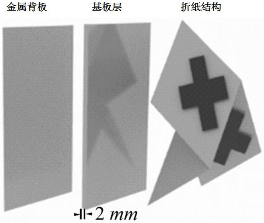
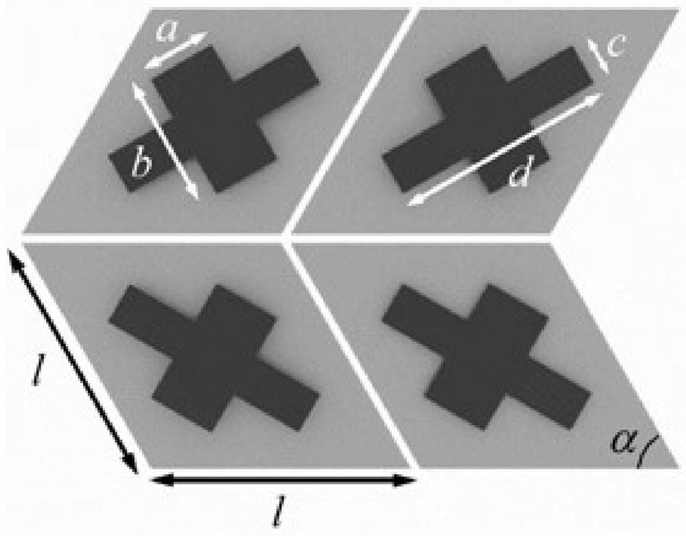
[0027] A three-dimensional reconfigurable broadband wide-angle absorbing material (hereinafter or simply referred to as an absorbing material), such as figure 1 As shown, the origami structure, a substrate layer, and a metal back panel sequentially provided in the direction of electromagnetic propagation, including a reconstigrable substrate and a super material structure unit printed on the reconfigurable substrate.

[0028] In this embodiment, the reconstiguentity substrate is a polyimide substrate having a thickness of 0.05 mm. The mater...


PUM

PropertyMeasurementUnit
thicknessaaaaaaaaaa
thicknessaaaaaaaaaa

Abstract

The invention belongs to the technical field of stealth materials, and relates to a three-dimensional reconfigurable broadband wide-angular-domain wave-absorbing material based on Miura origami. The material comprises an origami structure, a substrate layer and a metal back plate which are sequentially arranged in the electromagnetic propagation direction, and the origami structure comprises a reconfigurable substrate and a metamaterial structure unit printed on the reconfigurable substrate. According to the three-dimensional reconfigurable broadband wide-angular-domain wave-absorbing material based on the Miura origami of the invention, the wave-absorbing material can be dynamically adjusted, and ultra-wideband absorption of TM waves is realized by optimizing the structural design; and meanwhile, the reconfigurable wave-absorbing material has good oblique incidence performance and a wide angular domain. With continuous development of shape memory alloy, 4D printing, origami and other micro-manufacturing technologies, the material has a wider application space in manufacturing reconfigurable devices.

Description

Technical field [0001] The present invention belongs to the technical field of invasive materials, and in particular to a three-dimensional reconfigurable broadband wide-angle beam absorbing material based on three-purpose origami. Background technique [0002] In the context of information warfare, electromagnetic absorbing materials are one of the effective ways to achieve stealth technologies, and have become the focus of competition research. At the same time, it has broad application prospects in the fields of wireless communication, electromagnetic shielding and electromagnetic compatibility. In order to achieve efficient electromagnetic absorbing characteristics, conventional absorbing materials have conducted in-depth research on the physical and chemical properties of the components of the material, and prepared a series of suction with conductive losses, dielectric loss and magnetic loss characteristics. Wave material. However, with the study of the performance characte...

Claims


Application Information

Patent Timeline
Patent Type & Authority Applications(China)
IPC IPC(8): H01Q15/00H01Q17/00
CPCH01Q15/0086H01Q15/002H01Q17/007
Inventor 李勇峰朱志标屈绍波成洋秦喆郑麟王甲富
Owner AIR FORCE UNIV PLA
Why Eureka
Try Eureka