An ultra-low temperature wafer implantation platform

An ultra-low temperature, wafer technology, applied in the direction of discharge tubes, electrical components, circuits, etc., can solve problems such as the inability to form amorphous layers, and achieve the effect of suppressing the instantaneous enhanced diffusion effect

Active Publication Date: 2022-03-15
北京凯世通半导体有限公司
View PDF5 Cites 0 Cited by
  • Summary
  • Abstract
  • Description
  • Claims
  • Application Information

AI Technical Summary

Problems solved by technology

Because of the dynamic annealing phenomenon during normal temperature ion implantation or shallow low temperature ion implantation, normal temperature ion implantation or shallow low temperature ion implantation cannot form the required amorphous layer on the wafer surface well.

Method used


Image

  • An ultra-low temperature wafer implantation platform
  • An ultra-low temperature wafer implantation platform
  • An ultra-low temperature wafer implantation platform

Examples


Embodiment Construction

[0037] The technical solutions in the patent embodiments of the present invention will be clearly and completely described below in conjunction with the accompanying drawings in the patent embodiments of the present invention. Obviously, the described embodiments are only a part of the patent embodiments of the present invention, not all of them. Example. Based on the embodiments in the patent of the present invention, all other embodiments obtained by persons of ordinary skill in the art without making creative efforts belong to the protection scope of the patent of the present invention.

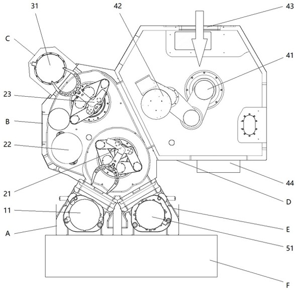
[0038] see figure 1 , a kind of ultra-low temperature wafer implantation platform provided by the present invention, at least includes a front-end wafer transfer module F, a loading module A, a vacuum transfer module B, a vacuum cooling module C, a vacuum injection module D and a vacuum heating module E, the front-end wafer transfer module Module F, loading module A, vacuum transfer modul...


PUM


Abstract

The invention provides an ultra-low temperature wafer injection platform. The ultra-low temperature wafer injection platform at least includes a front-end wafer transfer module, a loading module, a vacuum transfer module, a vacuum cooling module, a vacuum injection module, and a vacuum heating module. The front modules cooperate with each other and form a An organic whole; this organic whole realizes ultra-low temperature wafer ion implantation; in the vacuum cooling module, the wafer is cooled rapidly through the cooling platform for cooling the wafer and the electrostatic chuck for absorbing the wafer, so that the wafer is in an ultra-low temperature state, and the ultra-low temperature The temperature in the state is below minus 50 degrees Celsius. The present invention effectively suppresses the dynamic annealing in the ion implantation process, so that the interstitial position atoms can no longer return to the replacement position of the lattice, so that the number of amorphous packets increases and the range of amorphous packets gradually expands. Finally, the boundaries of all amorphous packets are connected at Form a complete amorphous layer together; the invention realizes ultra-low temperature ion implantation and forms a complete amorphous layer.

Description

technical field [0001] The invention belongs to the field of semiconductor manufacturing and processing, and relates to an ultra-low temperature wafer implantation platform, which is suitable for ion implantation equipment. Background technique [0002] Semiconductor devices have been developing toward miniaturization for a long time. According to Moore's Law, the number of semiconductor devices integrated on a unit area of ​​an integrated circuit chip will double every 18 months, and with the miniaturization of semiconductor devices , Most of the internal structures of semiconductor devices are bound to be scaled down proportionally. At present, the critical dimensions of semiconductor devices have reached the nanometer or deep nanometer level. How to manufacture ultra-shallow junctions and abrupt junctions in semiconductor devices, and how to more completely repair ion implantation end-of-range defects (EOR Damage) in the manufacturing process of semiconductor devices have...

Claims


Application Information

Patent Timeline
Patent Type & Authority Patents(China)
IPC IPC(8): H01J37/02H01J37/18H01J37/317H01L21/265H01L21/67
CPCH01J37/3171H01J37/18H01J37/02H01L21/67248H01L21/26593
Inventor 陈炯王振辉孙蒿泉康劲高国珺雷晓刚张彦彬李恒王辉卢合强刘金涛肖嘉星洪俊华关天祺
Owner 北京凯世通半导体有限公司
Why Eureka
Try Eureka