
Test circuit and test method for testing common source inductance of power device

A technology for power devices and power testing, which is used in electrical measurement, electrical variable measurement, and single semiconductor device testing. The effect of measurement

Active Publication Date: 2022-02-01
XI AN JIAOTONG UNIV +1
View PDF4 Cites 0 Cited by
  • Summary
  • Abstract
  • Description
  • Claims
  • Application Information

AI Technical Summary

Problems solved by technology

However, FEA extraction requires an accurate internal structure of the semiconductor package, otherwise the extracted CSI will have a certain deviation from the actual value
On the one hand, the manufacturer does not provide the internal structure of the device, which makes it difficult to use the FEA method; on the other hand, the common source inductance exists as a coupling part, and the decoupling between the power loop and the drive loop extracts the parasitic inductance requirements High, so the simulation extraction can not get the accurate value of the common source inductance

Method used

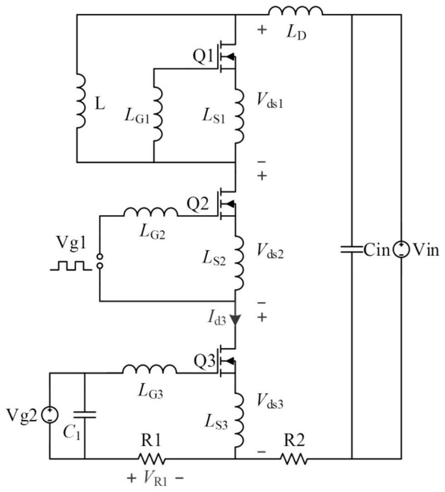
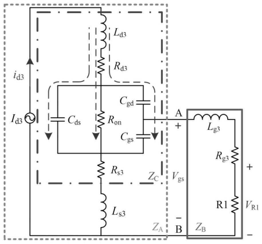

Image

  • Test circuit and test method for testing common source inductance of power device
  • Test circuit and test method for testing common source inductance of power device
  • Test circuit and test method for testing common source inductance of power device

Examples


Embodiment Construction

[0038] In order to make the purpose, technical solutions and advantages of the embodiments of the present invention clearer, the technical solutions of the present invention will be clearly and completely described below in conjunction with the accompanying drawings. Obviously, the described embodiments are part of the embodiments of the present invention, not all of them. the embodiment. Based on the embodiments of the present invention, all other embodiments obtained by persons of ordinary skill in the art without making creative efforts belong to the protection scope of the present invention.

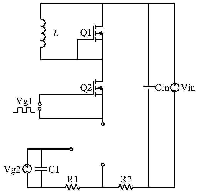
[0039] As a specific embodiment of the present invention, such as figure 1 As shown, a test circuit for testing the common source inductance of power devices, including power MOSFET Q1, power MOSFET Q2, inductor L, input capacitor Cin, pulse signal generator Vg1, driving voltage source Vg2, driving input capacitor C1, Test resistor R1, coaxial resistor R2 and input voltage source Vi...


PUM


Abstract

The invention discloses a test circuit and a test method for testing the common-source inductance of a power device, which can accurately measure the common-source inductance of the power device, can build the test circuit at low cost, and measures the common-source inductance of the device according to different packaging forms and sizes. Compared with a previous measurement mode, the test method provided by the invention not only can accurately measure the common-source inductance of the power device after the layout is determined, but also can measure the common-source inductance of the power device by considering the coupling effect between a power loop and a driving loop.

Description

technical field [0001] The technical field of power electronics of the present invention relates in particular to a test circuit and a test method for testing common source inductance of power devices. Background technique [0002] Wide bandgap semiconductor devices, such as SiC-MOSFETs and GaN-HEMTs, are rapidly developing due to their excellent switching characteristics and lower on-resistance compared with conventional Si-MOSFETs, and are considered to be the most promising power devices , can be used to improve the efficiency and power density of power converters. However, as the switching frequency increases, some problems due to parasitic parameters become more serious, such as false triggering, increased switching losses, and voltage overshoots. The common source inductance, as the coupling part of the power loop and the drive loop, is considered to be the main reason for increasing the switching loss, destroying the switching characteristics of the power device and ...

Claims


Application Information

Patent Timeline
Patent Type & Authority Applications(China)
IPC IPC(8): G01R31/26
CPCG01R31/2621Y02B70/10
Inventor 吴佳芮杨旭王康平陈文洁魏吉文魏高昊陈桥梁
Owner XI AN JIAOTONG UNIV
Learn More