High-frequency waveguide assembly with welding flux overflow suppression structure and welding method
A high-frequency wave and solder technology, applied to waveguide devices, waveguides, welding equipment, etc., can solve problems such as solder shortage on the welding surface, solder accumulation in the waveguide cavity, and disordered solder flow, so as to reduce solder flow and optimize thickness and flatness , Use the effect that the performance is not affected
- Summary
- Abstract
- Description
- Claims
- Application Information
AI Technical Summary
Problems solved by technology
Method used
Image
Examples
Embodiment 1
[0055] Embodiment 1 takes a waveguide power splitter as an example.
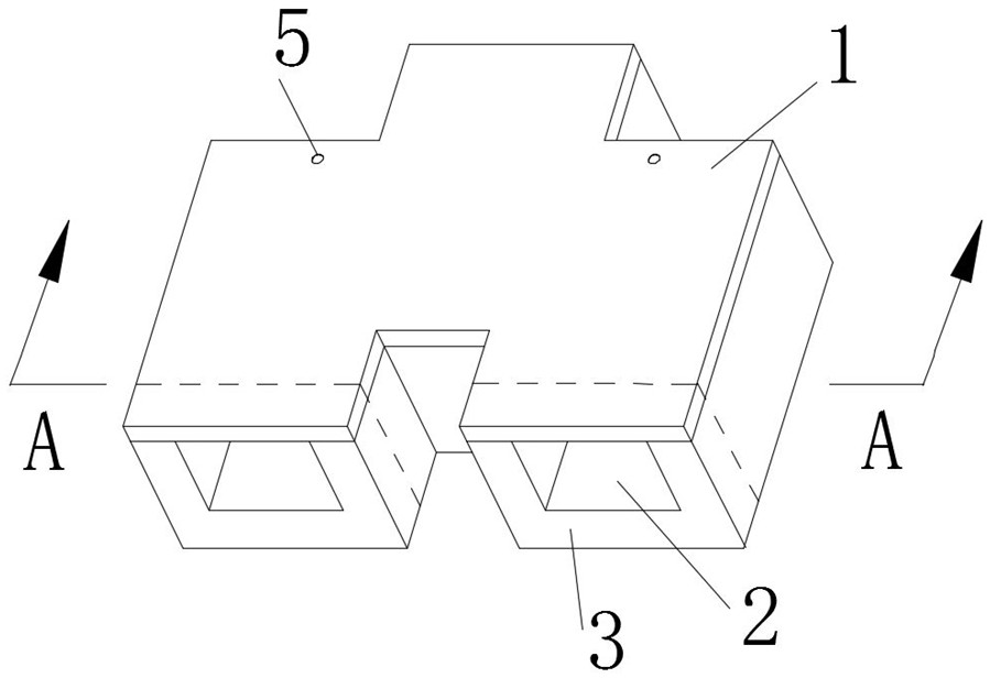
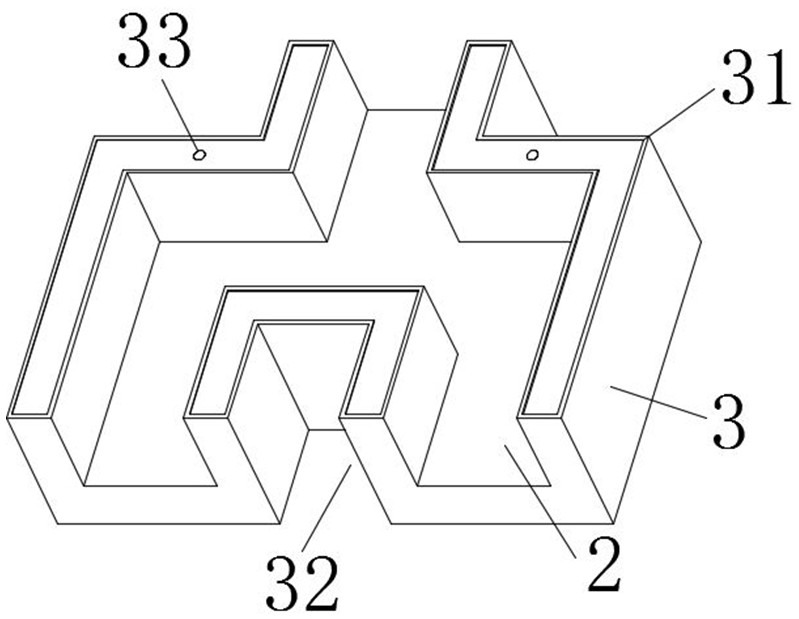
[0056] see figure 1 , the waveguide power splitter includes a cover plate 1 and a waveguide shell 3 . In order to prevent the solder piece 4 from flowing into the waveguide cavity 2 after melting, the waveguide shell 3 has been improved in technology; see figure 2 The waveguide housing 3 is provided with a waveguide cavity 2, the top surface of the waveguide housing 3 is a welding surface, the welding surface is provided with a solder resist dam 31, and the solder resist dam 31 forms a closed area along the contour of the welding surface.
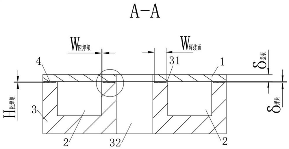
[0057] The width of the welding surface between adjacent solder resist dams 31 on the waveguide shell should be selected properly; on the premise of ensuring the welding quality, the welding area should be reduced to control the disordered flow of solder. The width of the welding surface is twice the thickness of the cover plate.
[0058] see image 3 , the solder re...
Embodiment 2
[0072] see Figure 5 and Figure 6 , Embodiment 2 takes a certain waveguide cavity component as an example.
[0073] see Figure 5 and Figure 7 The shape of the contact welding surface between the waveguide shell 3 and the cover plate 1 is complex and the width is large. Firstly, the hollow area 32 is designed for the area with a large thickness, so as to reduce the welding area. The width of the welding surface is twice the thickness of the cover plate, and the overly wide part of the waveguide housing 3 is hollowed out to remove the material in the hollowed out area 32 so that the width of the welding surface meets the technical requirements. see Figure 6 , the top surface of the waveguide housing 3 is a welding surface, and the welding surface is provided with a solder resist dam 31 , and the solder resist dam 31 forms a closed area along the contour of the weld surface.
[0074] The height H of the solder resist dam 31 阻焊坝 The setting should avoid the shortage of s...
PUM
| Property | Measurement | Unit |
|---|---|---|
| surface smoothness | aaaaa | aaaaa |
| surface smoothness | aaaaa | aaaaa |
| thickness | aaaaa | aaaaa |
Abstract
Description
Claims
Application Information


