
Direct-insertion part tinning optimization welding method and system

A welding method and parts technology, which is applied in the field of servers, can solve problems such as time-consuming and labor-intensive, poor welding, non-standard, etc.

Pending Publication Date: 2022-02-15
SUZHOU LANGCHAO INTELLIGENT TECH CO LTD
View PDF7 Cites 0 Cited by
  • Summary
  • Abstract
  • Description
  • Claims
  • Application Information

AI Technical Summary

Problems solved by technology

Compared with SMD parts, the size and structure of in-line parts are much more complicated, and they are not standard and irregular. Each manufacturer can basically only guarantee that the function meets the standard, but the specific size cannot be unified.
[0005] Since the thickness of the pins of the in-line parts is different, and the opening diameters of the installation through holes on the board PCB produced by different manufacturers are also different, so the opening of the installation through holes often occurs in the production process. The diameter is much larger than the diameter of the pins of the in-line parts, which leads to the fact that the pins are too far away from the inner wall of the mounting through hole during wave soldering of the in-line parts, and it is difficult for liquid solder (liquid tin, etc.) to crawl between the two. Filling, leading to soldering quality problems such as insufficient tin amount and poor soldering
In the prior art, it is generally only possible to manually correct each installation through-hole at the end of the wave soldering process, such as manual soldering, solder repair, etc., but the number of installation through-holes is too large, which leads to time-consuming and laborious. The labor load of the workers is too large, which not only affects the production efficiency but also easily leads to unqualified welding quality
[0006] Therefore, how to increase the amount of tin on the in-line parts in the wave soldering process, prevent the quality problems of poor soldering, and avoid manual repair work in the later stage is a technical problem faced by those skilled in the art.

Method used


Image

  • Direct-insertion part tinning optimization welding method and system
  • Direct-insertion part tinning optimization welding method and system
  • Direct-insertion part tinning optimization welding method and system

Examples


Embodiment Construction

[0051] The following will clearly and completely describe the technical solutions in the embodiments of the present invention with reference to the accompanying drawings in the embodiments of the present invention. Obviously, the described embodiments are only some, not all, embodiments of the present invention. Based on the embodiments of the present invention, all other embodiments obtained by persons of ordinary skill in the art without making creative efforts belong to the protection scope of the present invention.

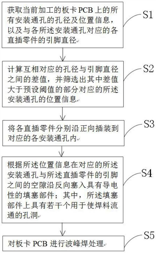
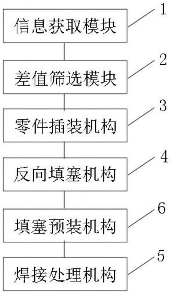
[0052] Please refer to figure 1 , figure 1 It is a method flowchart of a specific embodiment provided by the present invention.

[0053] In a specific embodiment provided by the present invention, the tin optimization soldering method on in-line parts mainly includes five steps, which are:

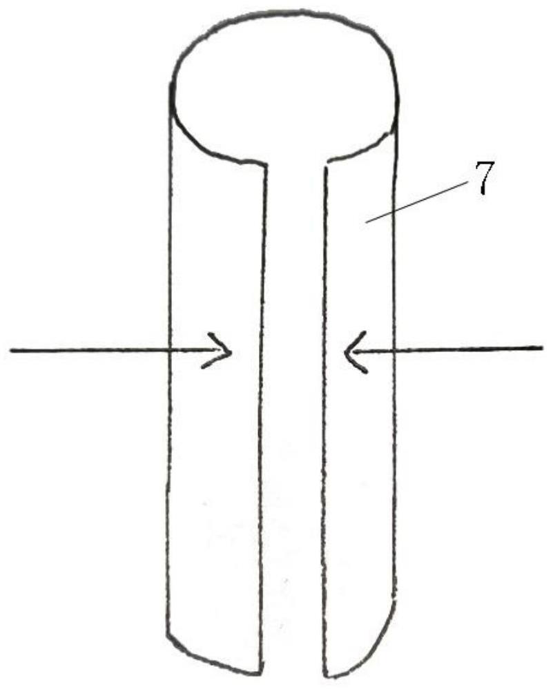
[0054] S1. Obtain the aperture and position information of all the installation through holes on the currently processed board PCB, and the pin diameters of the in-line ...


PUM


Abstract

The invention discloses a direct-insertion part tinning optimization welding method, which comprises the following steps of: acquiring the aperture and position information of all mounting through holes in a currently processed board card PCB, and the pin diameter of each direct-insertion part corresponding to each mounting through hole; calculating a difference value between the aperture and the pin diameter which correspond to each other, and screening out the position information of the mounting through hole corresponding to the part of which the difference value is greater than a preset threshold value; inserting direct-insertion parts into the corresponding mounting through holes in the forward direction; according to the position information, plugging filling parts with conductivity in gaps between the corresponding mounting through holes and the pins of the direct-insertion parts in the reverse direction, wherein a plurality of holes used for allowing welding flux to circulate are formed in the filling parts; and carrying out wave soldering processing on the board card PCB. According to the direct-insertion part tinning optimization welding method, the tinning amount of the direct-insertion parts in the wave soldering process can be improved, the quality problem of poor soldering is prevented, and the later manual repair work is avoided. The other purpose of the invention is to provide a direct-insertion part tinning optimization welding system.

Description

technical field [0001] The invention relates to the technical field of servers, in particular to an optimized tin welding method for in-line parts. The invention also relates to a tin optimization welding system for in-line parts. Background technique [0002] With the increase in the types of personal electronic consumer products and the development of various data clouds, the application range of servers and personal electronic consumer products is becoming wider and wider. Among them, large-scale public cloud operators continue to deploy infrastructure as the main force to drive growth, so as to facilitate home office or online teaching, as well as increased demand for online business, and these activities will become the norm in the future, resulting in servers and personal electronic consumer products. more and more. [0003] The increase in the number of servers and personal electronic consumer products has led to an increasing demand for boards in the electronics in...

Claims


Application Information

Patent Timeline
IPC IPC(8): B23K1/08B23K3/00B23K3/08B23K37/04
CPCB23K1/085B23K3/00B23K3/08B23K3/087B23K2101/42
Inventor 于浩
Owner SUZHOU LANGCHAO INTELLIGENT TECH CO LTD
Features
  • Generate Ideas
  • Intellectual Property
  • Life Sciences
  • Materials
  • Tech Scout
  • Unparalleled Data Quality
  • Higher Quality Content
  • 60% Fewer Hallucinations
Learn More