Flexible touch function film with color display function
A flexible touch and color display technology, applied in the input/output process of data processing, instruments, electrical digital data processing, etc. Logo layer and other problems, to achieve the effect of reducing the pasting process, saving labor consumption, and improving touch stability
- Summary
- Abstract
- Description
- Claims
- Application Information
AI Technical Summary
Problems solved by technology
Method used
Image
Examples
Embodiment 1
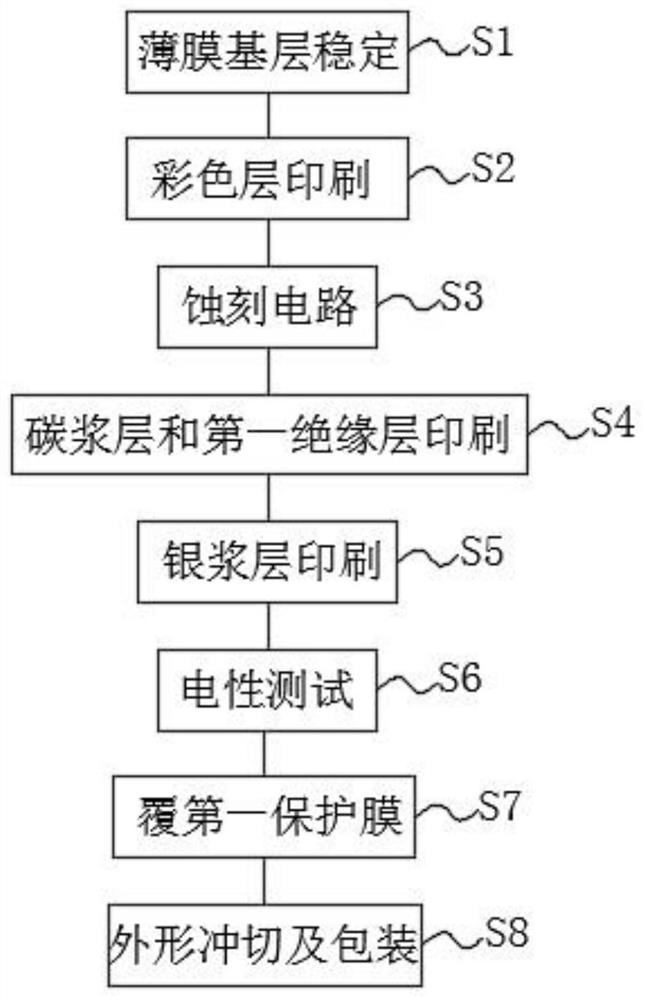
[0030] Embodiment 1: as figure 1 and image 3 As shown, the present invention provides a flexible touch functional film for color display, comprising a film base layer 10, one side of the film base layer 10 is fixed with a printed color layer 11, the other side of the film base layer 10 is fixed with a printed etching circuit layer 12, and the etching circuit A plurality of carbon paste layers 13 are printed on the layer 12, and the first insulating layer 14 is printed on the etching circuit layer 12 outside the carbon paste layer 13, and the first insulating layer 14 is away from the fixed printing silver paste layer 15 on the side of the etching circuit layer 12. The paste layer 15 is electrically in contact with the carbon paste layer 13 , and the side of the silver paste layer 15 away from the first insulating layer 14 is fixedly printed with the second insulating layer 16 . The color layer 11 of the touch button is directly printed on one side of the film base layer 10, ...
Embodiment 2
[0045] Example 2: see figure 2 , the difference from Example 1 is that one side of the film base layer 10 is fixedly printed with a colored layer 11, and the side of the colored layer 11 away from the film base layer 10 is fixedly printed with an etched circuit layer 12, and a plurality of carbon paste layers are printed on the etched circuit layer 12 13. The first insulating layer 14 is printed on the etched circuit layer 12 outside the carbon paste layer 13, and the side of the first insulating layer 14 away from the etched circuit layer 12 is fixedly printed with a silver paste layer 15, and the silver paste layer 15 is electrically in contact with the carbon paste layer 13. The side of the silver paste layer 15 away from the first insulating layer 14 is fixedly printed with the second insulating layer 16, and the side of the film base layer 10 away from the color layer 11 is fixedly adhered to the second protective film 18, and the second insulating layer 16 is away from t...
PUM
| Property | Measurement | Unit |
|---|---|---|
| thickness | aaaaa | aaaaa |
Abstract
Description
Claims
Application Information


