Mask layer rework method and silicon nitride etching method

A mask layer and silicon nitride layer technology, applied in semiconductor/solid-state device testing/measurement, electrical components, circuits, etc., can solve problems such as substrate retention, etching end-time alarm, and substrate scrapping.

Active Publication Date: 2022-04-15
GUANGZHOU CANSEMI TECH INC
View PDF6 Cites 0 Cited by
  • Summary
  • Abstract
  • Description
  • Claims
  • Application Information

AI Technical Summary

Problems solved by technology

However, in the dry etching of the substrate of the above-mentioned heavy mask layer, the etch end time alarm (for example, the etch end time is overtime) often occurs, causing the substrate to stay in the dry etching machine, which not only affects the production cycle, but also affects the substrate. The introduction of more defects on the bottom affects product quality, and there is even a risk of completely scrapping the substrate

Method used


Image

  • Mask layer rework method and silicon nitride etching method
  • Mask layer rework method and silicon nitride etching method
  • Mask layer rework method and silicon nitride etching method

Examples


Embodiment Construction

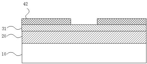
[0024] Such as figure 1 As shown, after analyzing the substrate 10 with the reworked mask layer, the inventor found that there is a first silicon oxynitride layer 31 on the silicon nitride layer 20 under the patterned mask layer 42 . In the process of reworking the mask layer, the silicon nitride layer 20 is partially (partially thick) oxidized into a first silicon oxynitride layer 31 in an ashing process for removing the mask layer. In the subsequent etching of the silicon nitride layer, the etch rate of the first silicon oxynitride layer 31 is different from the etch rate of the silicon nitride layer 20, thus causing an alarm due to an abnormal etch end time of the substrate 10 after the reworked mask layer ( different from the substrate without the reworked mask layer), which in turn causes the substrate 10 to stay in the dry etching machine.

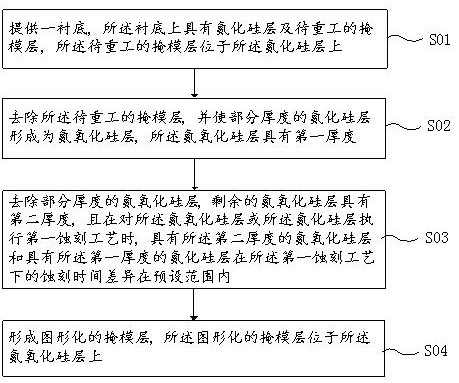
[0025] Based on the above research of the inventors, an embodiment of the present invention provides a mask layer rework method, b...


PUM

PropertyMeasurementUnit
thicknessaaaaaaaaaa
thicknessaaaaaaaaaa

Abstract

The invention provides a method for reworking a mask layer and a method for etching silicon nitride. The method for reworking the mask layer includes: providing a substrate; removing the mask layer to be reworked, and making the silicon nitride layer partially thick Formed as a silicon oxynitride layer; part of the thickness of the silicon oxynitride layer is removed, and when the first etching process is performed on the silicon oxynitride layer or the silicon nitride layer, the silicon oxynitride layer with the second thickness and the silicon oxynitride layer with the first thickness The etching time difference of the silicon nitride layer under the first etching process is within a preset range; a patterned mask layer is formed. In the present invention, by removing part of the thickness of the silicon oxynitride layer, the difference in etching time between the silicon oxynitride layer with the second thickness and the silicon nitride layer with the first thickness during etching by the first etching process is within a preset range In order to solve the problem of alarming in dry etching of the silicon nitride layer behind the reworked mask layer.

Description

technical field [0001] The invention relates to the technical field of semiconductors, in particular to a mask layer rework method and a silicon nitride etching method. Background technique [0002] In semiconductor technology, silicon nitride is a common dielectric material, and its application is very extensive. [0003] Take the patterning (dry etching) process of the silicon nitride layer as an example: a silicon nitride layer is formed on the substrate, a patterned mask layer is formed on the silicon nitride layer, and then the silicon nitride layer is dry etched to A patterned silicon nitride layer is formed, and the formation process of the silicon nitride layer is monitored (monitored) using the etching end time during the dry etching process. [0004] Wherein, after the patterned mask layer is formed, the patterned mask layer needs to be inspected for appearance, to prevent the substrate of the patterned mask layer with appearance defects from flowing into the dry ...

Claims


Application Information

Patent Timeline
Patent Type & Authority Patents(China)
IPC IPC(8): H01L21/311H01L21/66
CPCH01L21/31144H01L21/31116H01L22/26H01L22/12
Inventor 廖军张志敏
Owner GUANGZHOU CANSEMI TECH INC
Why Eureka
Try Eureka