Supercharge Your Innovation With Domain-Expert AI Agents!

Wafer bearing box

A carrier sheet and carrier technology, which is applied in the manufacture of electrical components, semiconductor/solid-state devices, circuits, etc., can solve problems such as surface damage, glossiness not meeting the requirements, and affecting product quality, so as to avoid damage and avoid corrosion cleaning The effect of different degrees and uniform shape around

Pending Publication Date: 2022-02-18
XUZHOU XINJING SEMICON TECH CO LTD +1
View PDF0 Cites 0 Cited by
  • Summary
  • Abstract
  • Description
  • Claims
  • Application Information

AI Technical Summary

Problems solved by technology

[0002] It is pointed out in related technologies that pollution, surface damage, and glossiness do not meet the requirements after silicon wafer slicing, which will affect product quality.
It needs to be etched and cleaned, and the silicon wafers placed in the silicon wafer box for etching and cleaning cannot ensure that the surrounding morphology of the silicon wafers is uniform and the thickness is the same

Method used


Image

  • Wafer bearing box
  • Wafer bearing box
  • Wafer bearing box

Examples


Embodiment Construction

[0032] Embodiments of the present invention are described in detail below, examples of which are shown in the drawings, wherein the same or similar reference numerals designate the same or similar elements or elements having the same or similar functions throughout. The embodiments described below by referring to the figures are exemplary and are intended to explain the present invention and should not be construed as limiting the present invention.

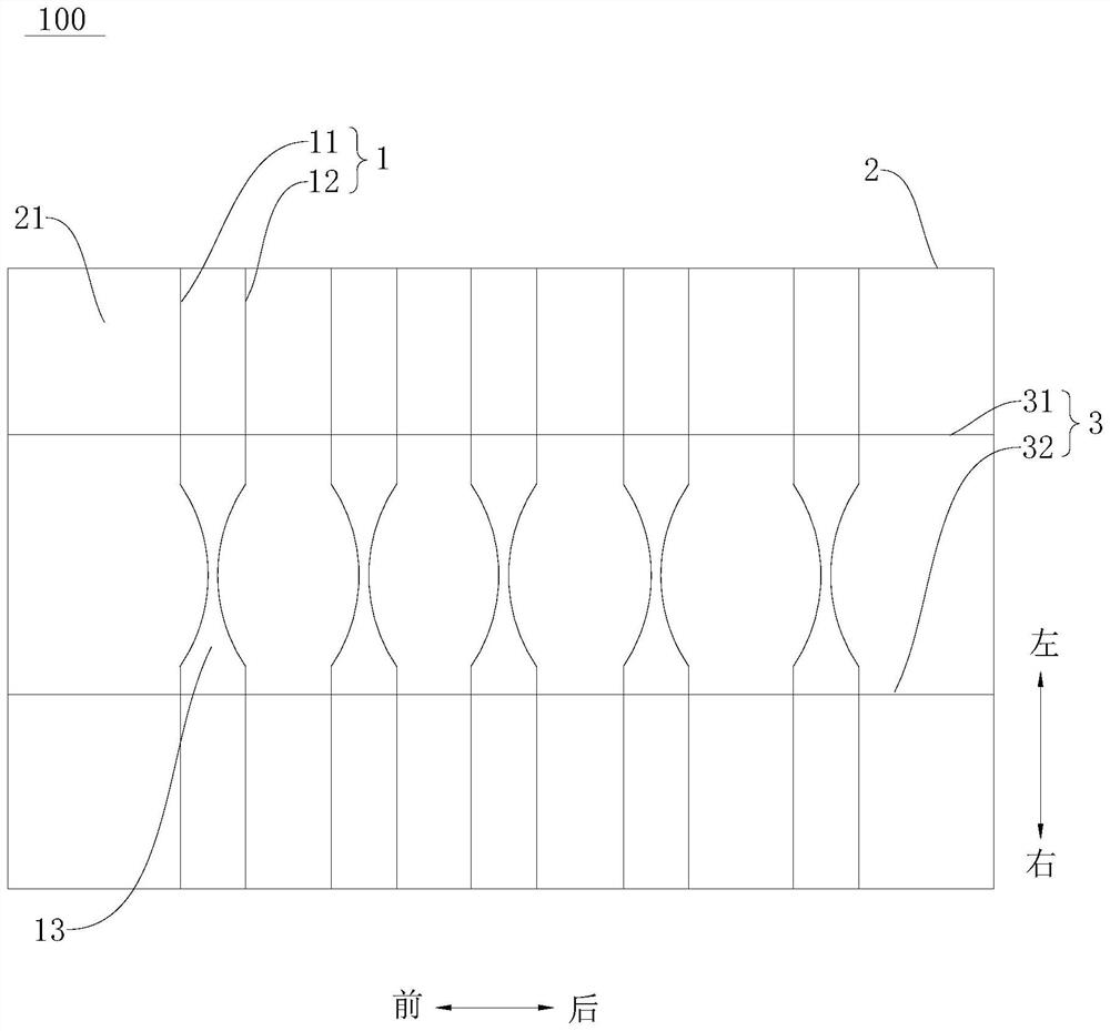
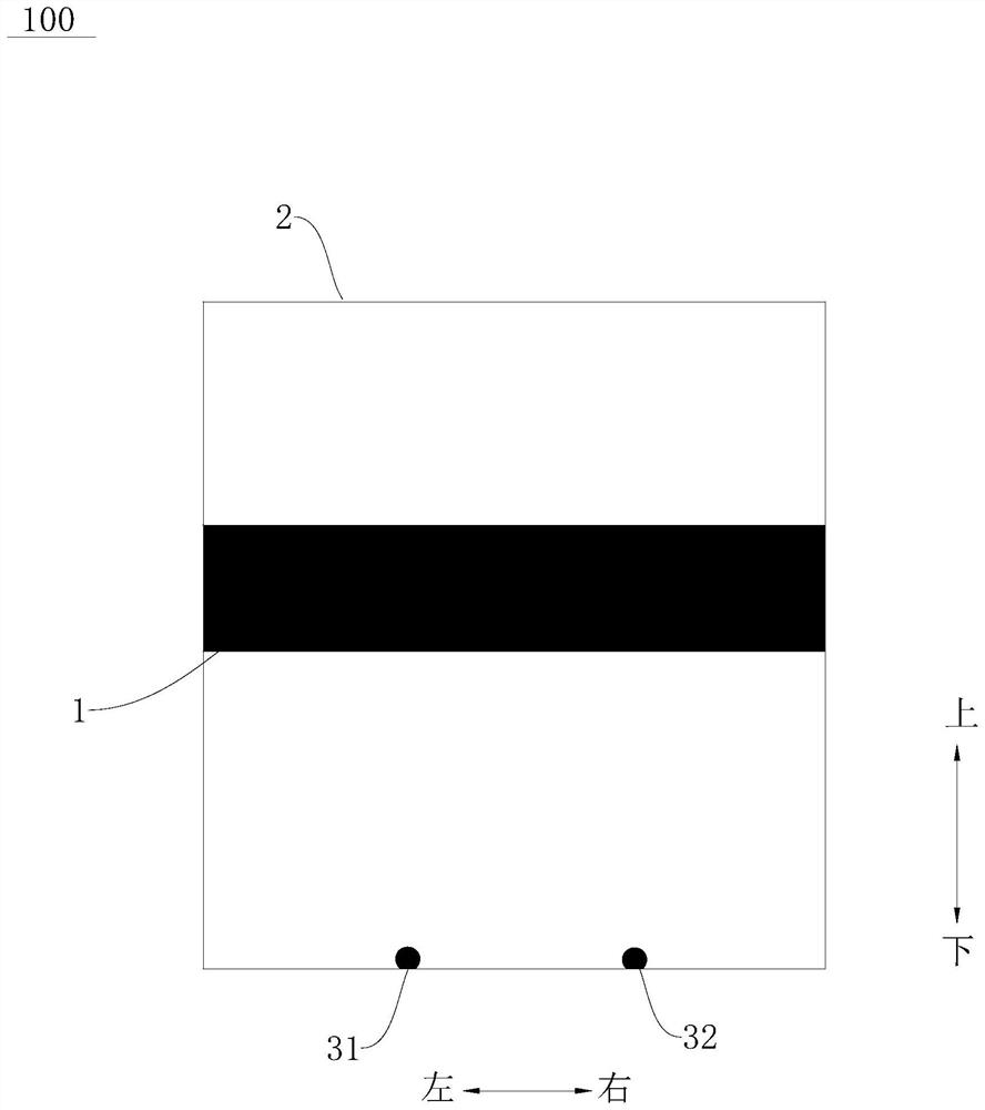
[0033] Refer below Figure 1-Figure 3 A carrier sheet cassette 100 according to an embodiment of the first aspect of the present invention will be described.

[0034] like figure 1 As shown, the carrier cassette 100 according to the embodiment of the first aspect of the present invention includes a carrier frame.

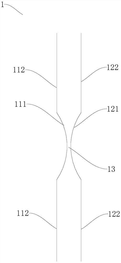
[0035] Specifically, the carrier includes a clamping arm 1, and the clamping arm 1 includes a first clamping arm 11 and a second clamping arm 12 arranged at intervals in the horizontal direction, and a boundary betwe...


PUM

PropertyMeasurementUnit
diameteraaaaaaaaaa
diameteraaaaaaaaaa
thicknessaaaaaaaaaa

Abstract

The invention discloses a wafer bearing box. The wafer bearing box comprises a bearing frame, the bearing frame comprises clamping arms, the clamping arms comprise a first clamping arm and a second clamping arm which are arranged at intervals in the horizontal direction, a clamping space is defined between the first clamping arm and the second clamping arm, a silicon wafer is suitable for being placed in the clamping space, and the first clamping arm and the second clamping arm abut against the surfaces of the two sides of the silicon wafer in the thickness direction. According to the wafer bearing box, the first clamping arm and the second clamping arm are arranged at intervals in the horizontal direction, and the first clamping arm and the second clamping arm abut against the surfaces of the two sides of the silicon wafer in the thickness direction, so that the edge of the silicon wafer does not make contact with the bearing frame, and the situation that the corrosion cleaning degrees of the edge of the silicon wafer are different is avoided, therefore, the peripheral morphology of the edge of the silicon wafer is uniform, and damage caused by contact between the edge of the silicon wafer and the bearing frame is avoided.

Description

technical field [0001] The invention relates to the technical field of semiconductors, in particular to a carrying sheet box. Background technique [0002] It is pointed out in related technologies that after slicing silicon wafers, pollution, surface damage, and glossiness do not meet the requirements, etc., which affect product quality. It needs to be etched and cleaned, and the silicon wafers placed in the silicon wafer box for etching and cleaning cannot ensure that the surrounding morphology of the silicon wafers is uniform and the thickness is the same. Contents of the invention [0003] The present invention aims to solve at least one of the technical problems existing in the prior art. For this reason, the present invention is to provide a carrying sheet box, the carrying sheet box has a simple structure, which is beneficial to the uniform appearance of the surrounding area during silicon wafer etching and cleaning. [0004] According to the carrier film box of t...

Claims


Application Information

Patent Timeline
Patent Type & Authority Applications(China)
IPC IPC(8): H01L21/673
CPCH01L21/6732
Inventor 李向阳陈俊宏
Owner XUZHOU XINJING SEMICON TECH CO LTD
Features
  • R&D
  • Intellectual Property
  • Life Sciences
  • Materials
  • Tech Scout
  • Unparalleled Data Quality
  • Higher Quality Content
  • 60% Fewer Hallucinations
Learn More