Micro-energy acquisition circuit, acquisition device and power supply method
A technology for collecting circuits and micro-energy, applied to circuit devices, battery circuit devices, current collectors, etc., can solve problems such as low overall efficiency, large chances of using backup batteries, and insufficient battery charging cycles
- Summary
- Abstract
- Description
- Claims
- Application Information
AI Technical Summary
Problems solved by technology
Method used
Image
Examples
Embodiment 1
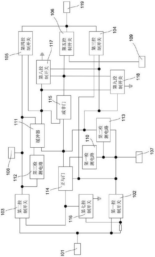
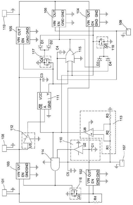
[0062] Example 1, see figure 1 with figure 2 .
[0063] A micro energy collection circuit, comprising an input port 101, a first control switch, a second control switch 103, a third control switch 104, a fourth control switch 105, a fifth control switch 106, and a first control switch for connecting to a first charge storage A charge storage port 107, a second charge storage port 108 for connecting the second charge storage, a third power supply port 109, a first detection circuit 110, a buffer 111, a third detection circuit 112, a second detection circuit 113, a positive AND gate 114, NOR gate 115, seventh control switch 116, eighth control switch 117, ninth control switch 118 and output port 119;
[0064] The first control switch, when the seventh control switch 116 is turned on, the first control switch is turned off; when the seventh control switch 116 is turned off, the first control switch receives input from the input port 101 and outputs to the first charge storage ...
Embodiment 2
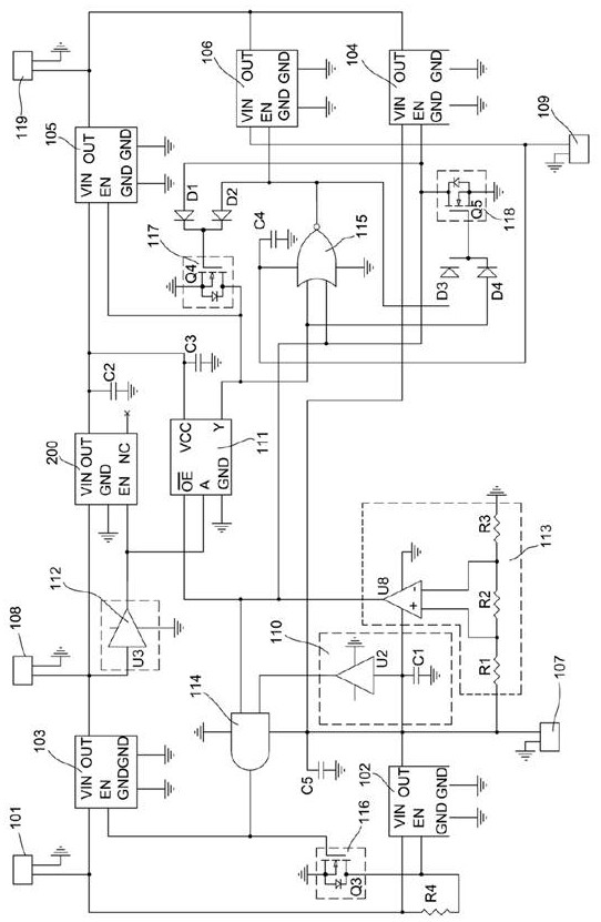
[0092] Example 2, see image 3 .
[0093] In this embodiment, a low dropout voltage regulator 200 is also included, the second charge storage port 108 is connected to the fourth control switch 105 through the low dropout voltage regulator 200, and when the control terminal of the low dropout voltage regulator 200 receives the ninth control signal Output, stop output when receiving the tenth control signal.
[0094] The input end of the low dropout voltage regulator 200 is connected with the output end of the second control switch 103; the input end of the fourth control switch 105 and the power supply pin of the buffer 111 are all connected with the output end of the low dropout voltage regulator 200; The control terminal of the differential voltage regulator 200 and the input terminal of the buffer 111 are connected to the output terminal of the third detection circuit 112 , and the output terminal of the low dropout voltage regulator 200 is connected to a second capacitor C...
Embodiment 3
[0097] Example 3, see Figure 4 .
[0098] In this embodiment, a DC conversion circuit is arranged at the back end of the input port 101 to boost the voltage as the output of the input port 101 .
[0099] The DC conversion circuit is a DC / DC conversion circuit 300, including a DC / DC converter U1; the EN pin and the VIN pin of the DC / DC converter U1 pass through a filter circuit and an input port formed by a fifth resistor R5 and a seventh capacitor C7 101 is connected; the SW pin of the DC / DC converter U1 is connected to the input port 101 after passing through an inductor L1. The FB pin and OUT pin of the DC / DC converter U1 pass through the output circuit composed of the sixth resistor R6, the seventh resistor R7 and the sixth capacitor C6, etc., and simultaneously connect with the input end of the first control switch 102 and the second control switch 103 input connection.
PUM
 Abstract
Description
Claims
Application Information


