Method for screening aberration sensitivity of optical system

A technology of optical system and sensitivity, applied in the field of optical system, can solve the problem of slow distribution of wave aberration

Pending Publication Date: 2022-03-01
NANJING CHENGXIN INTEGRATED CIRCUIT TECH RES INST CO LTD
View PDF0 Cites 0 Cited by
  • Summary
  • Abstract
  • Description
  • Claims
  • Application Information

AI Technical Summary

Problems solved by technology

[0004] The purpose of the present invention is to provide a method for screening the aberration sensitivity of the optical system, aiming to solve the problem that the traditional wave aberration control method obtains the wave aberration distribution at a slow speed

Method used


Image

  • Method for screening aberration sensitivity of optical system
  • Method for screening aberration sensitivity of optical system
  • Method for screening aberration sensitivity of optical system

Examples


Embodiment Construction

[0036] Embodiments of the present invention are described in detail below, examples of which are shown in the drawings, wherein the same or similar reference numerals designate the same or similar elements or elements having the same or similar functions throughout. The embodiments described below by referring to the figures are exemplary and are intended to explain the present invention and should not be construed as limiting the present invention.

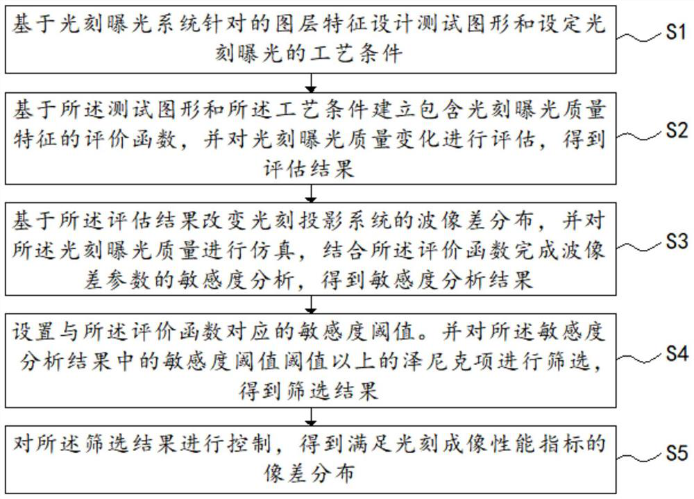
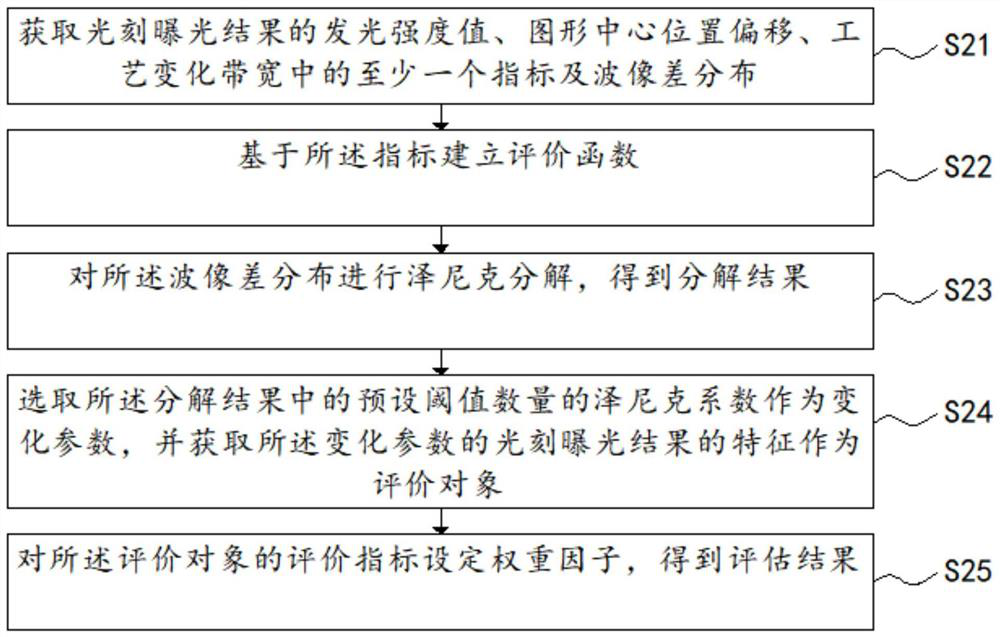
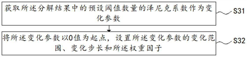
[0037] see Figure 1 to Figure 9 , the present invention provides a kind of method for screening optical system aberration sensitivity, comprising the following steps:

[0038] S1. Design test patterns based on the layer characteristics targeted by the lithography exposure system and set the process conditions for lithography exposure;

[0039] The process conditions include the lithography system type, wavelength, numerical aperture, polarization state, lithography process stack information, etc., the layer targeted by the lith...


PUM


Abstract

The invention relates to the technical field of optical systems, in particular to a method for screening aberration sensitivity of an optical system, which comprises the following steps of: designing a test pattern based on pattern layer characteristics of a photoetching exposure system, setting photoetching exposure process conditions and establishing an evaluation function containing photoetching exposure quality characteristics; evaluating the photoetching exposure quality change to obtain an evaluation result; changing wave aberration distribution of the photoetching projection system based on the evaluation result, simulating photoetching exposure quality, and completing sensitivity analysis of wave aberration parameters in combination with an evaluation function to obtain a sensitivity analysis result; setting a sensitivity threshold value corresponding to the evaluation function, and screening Zernike items above the threshold value in the sensitivity analysis result to obtain a screening result; the screening result is controlled to obtain aberration distribution meeting the photoetching imaging performance index, and the problem that the speed of obtaining the wave aberration distribution is low through a traditional wave aberration control method is solved.

Description

technical field [0001] The invention relates to the technical field of optical systems, in particular to a method for screening the aberration sensitivity of an optical system. Background technique [0002] Photolithography is a key technology in the manufacture of integrated circuits, responsible for transferring mask patterns onto silicon wafers. Similar to typical optical systems such as telescopes and microscopes, the lithography system uses projection imaging to shrink the graphic information on the mask onto the silicon wafer. In order to achieve accurate imaging of nanometer-sized patterns, the wave aberration of the lithographic projection optical system needs to have an extremely small range and extremely high control precision. Therefore, realizing precise control of wave aberration is of great value and significance for the development of lithography equipment and semiconductor manufacturing. [0003] The traditional wave aberration control methods all propose c...

Claims


Application Information

Patent Timeline
Patent Type & Authority Applications(China)
IPC IPC(8): G03F7/20
CPCG03F7/706G03F7/705
Inventor 刘畅董立松张世鑫韦亚一
Owner NANJING CHENGXIN INTEGRATED CIRCUIT TECH RES INST CO LTD
Why Eureka
Try Eureka