Waveguide interface structure

A waveguide interface and waveguide technology, which is applied to waveguide devices, electrical components, circuits, etc., can solve the problems of not being able to adapt to the use scene, the difficulty of waveguide processing, the processing of waveguide end faces, and high requirements for assembly, so as to solve the problem of non-coplanarity, Reduce the difficulty of structure processing and ensure the effect of normal signal transmission

Pending Publication Date: 2022-03-01
ZTE CORP
View PDF0 Cites 0 Cited by
  • Summary
  • Abstract
  • Description
  • Claims
  • Application Information

AI Technical Summary

Problems solved by technology

[0003] The inventors have found that there are at least the following problems in the prior art: the solutions in the prior art have high requirements for waveguide end surface processing and assembly, and the waveguide structure is difficult to process, and can only adapt to the situation of small interconnection gaps, and cannot adapt to large The usage scenario of the gap random tolerance

Method used


Image

  • Waveguide interface structure
  • Waveguide interface structure
  • Waveguide interface structure

Examples


Embodiment Construction

[0020] In order to make the purpose, technical solutions and advantages of the embodiments of the present invention more clear, various implementation modes of the present invention will be described in detail below in conjunction with the accompanying drawings. However, those of ordinary skill in the art can understand that, in each implementation manner of the present invention, many technical details are provided for readers to better understand the present application. However, even without these technical details and various changes and modifications based on the following implementation modes, the technical solution claimed in this application can also be realized.

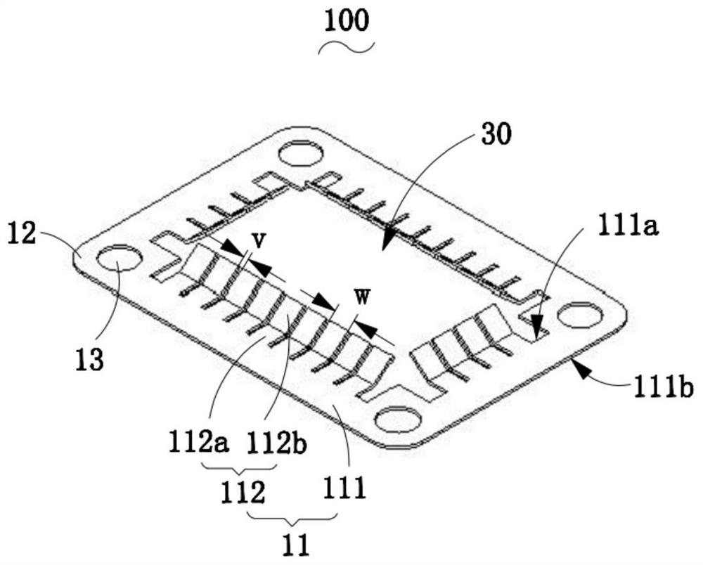
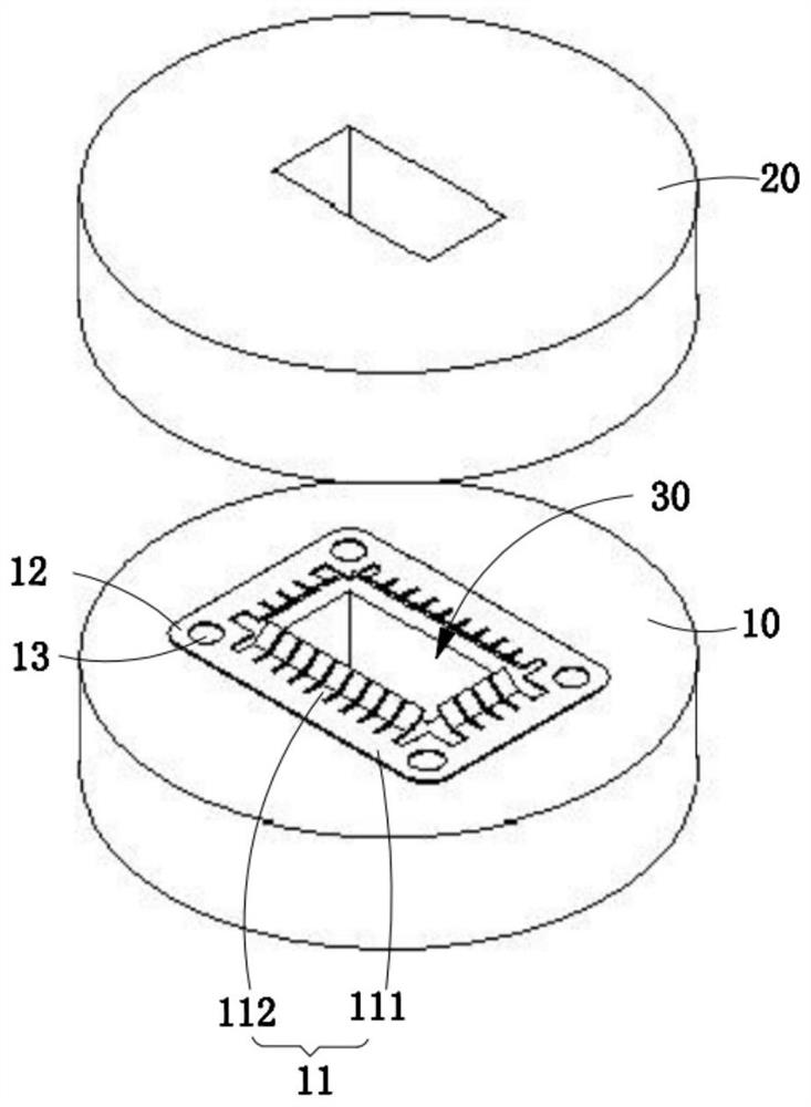
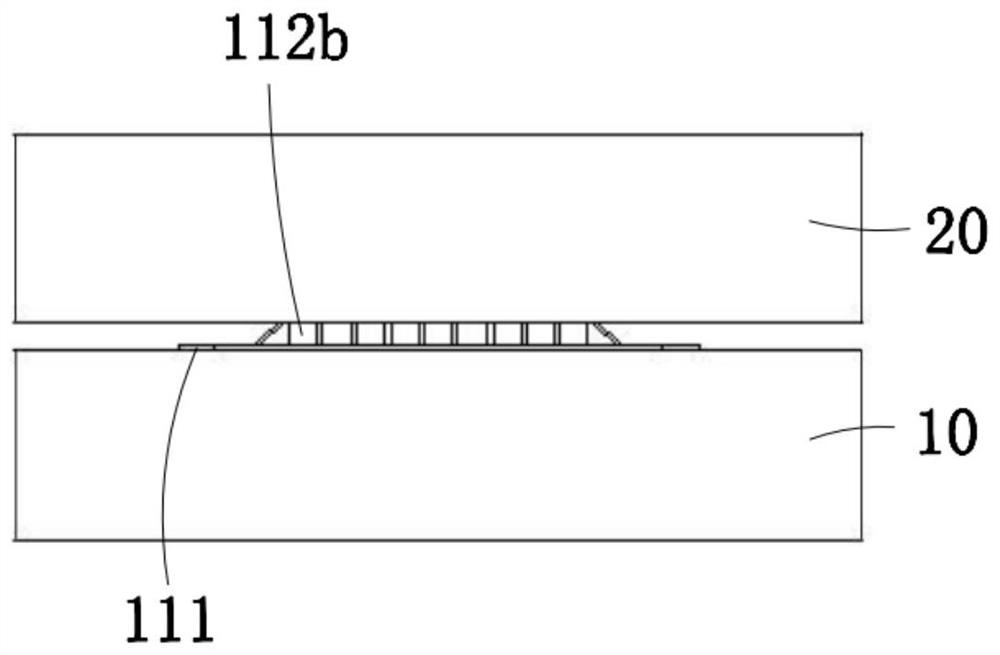
[0021] see Figure 1 to Figure 9 , the first embodiment of the present invention relates to a waveguide interface structure 100 for electrically connecting the first waveguide 10 and the second waveguide 20 . The core of this embodiment is that the waveguide interface structure 100 includes: an elastic elec...


PUM


Abstract

The embodiment of the invention relates to the field of microwave communication, and discloses a waveguide interface structure. The waveguide interface structure provided by the embodiment of the invention is used for electrically connecting a first waveguide and a second waveguide, and comprises an elastic electric connection part and a fixing part connected with the electric connection part, the fixing part is used for abutting against the end face of the first waveguide, and the electric connection part is enclosed to form an opening through which electromagnetic waves pass. And the electric connection part is elastically pressed between the end face of the first waveguide and the end face of the second waveguide and is electrically connected with the first waveguide and the second waveguide. The waveguide interface structure provided by the embodiment of the invention can reduce the processing difficulty of the waveguide structure on the premise of ensuring the normal signal transmission of the waveguide interconnection channel, and is suitable for the use scene of large-gap random tolerance.

Description

technical field [0001] The embodiment of the present invention relates to the field of microwave communication, and in particular to a waveguide interface structure. Background technique [0002] In the microwave frequency band, the waveguide has the smallest transmission loss, and it is an irreplaceable type of transmission line to improve the power generation and receiving sensitivity of the microwave communication system. When there is a gap in the waveguide interconnection, strong radiation loss and interference will occur, affecting the normal operation of the system. In the existing technology, most of the waveguide interconnection schemes are single waveguide ports and the priority is to ensure electrical connection, that is, the end faces of the two interconnected waveguide ports are in close contact. When there is a small interconnection gap, it is generally used around the waveguide port. The solution of placing the shielding sealing ring to solve the problem of e...

Claims


Application Information

Patent Timeline
IPC IPC(8): H01P1/04
CPCH01P1/042
Inventor 李卓王靖张勇舒建讯张震
Owner ZTE CORP
Why Eureka
Try Eureka