Millimeter wave packaging antenna based on fan-out packaging technology
A packaging process, millimeter wave technology, applied in antennas, antenna parts, antenna supports/installation devices, etc., can solve the problems of reduced antenna transmission performance, large signal attenuation and attenuation, large signal transmission distance, etc. The effect of shortening transmission distance, reducing attenuation and loss, and improving transmission performance
- Summary
- Abstract
- Description
- Claims
- Application Information
AI Technical Summary
Problems solved by technology
Method used
Image

Examples
Embodiment 1
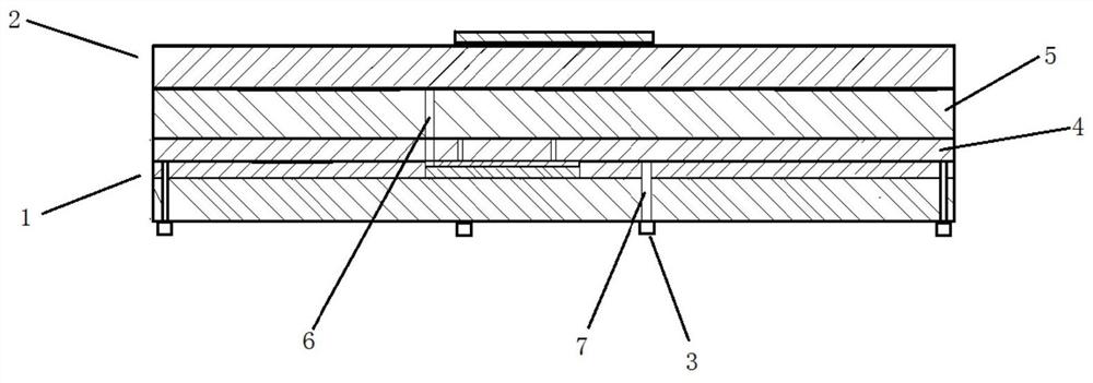
[0033] see figure 1 , this embodiment proposes a millimeter-wave packaged antenna based on fan-out packaging technology, including a chip package layer 1, an antenna radiation structure 2, an external substrate pad 3, a reflective metal layer 4, and a first passivation layer 5; The external substrate pad 3 is disposed under the chip packaging layer 1, the reflective metal layer 4 is disposed above the chip packaging layer 1; the first passivation layer 5 is disposed on the reflective metal layer 4 Above, the antenna radiation structure 2 is arranged above the first passivation layer 5; the antenna radiation structure 2 performs signal transmission with the chip packaging layer 1 through a conductor; the chip packaging layer 1 is soldered to the external substrate through a conductor Disc 3 performs signal transmission.
[0034] In the specific implementation process, the antenna radiation structure 2 directly performs signal transmission with the chip packaging layer 1 throug...
Embodiment 2
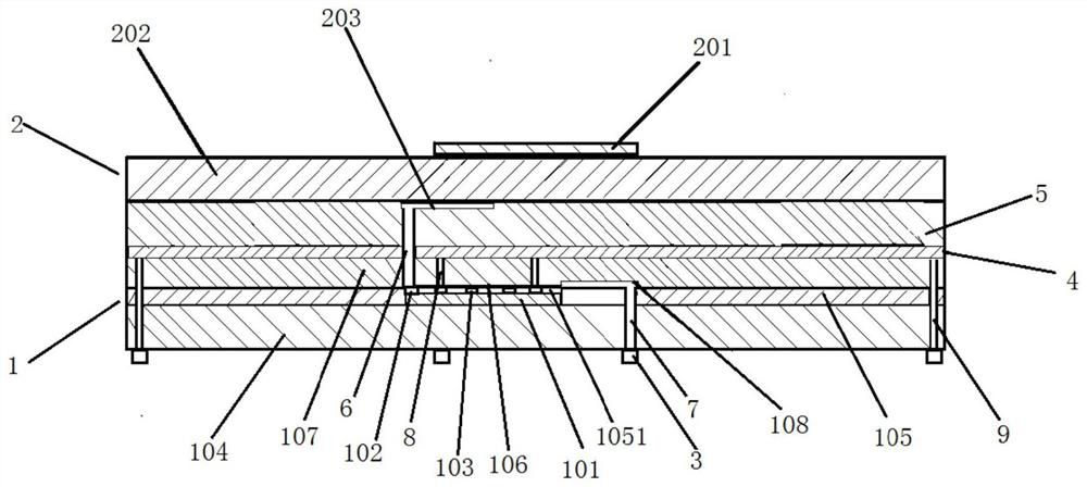
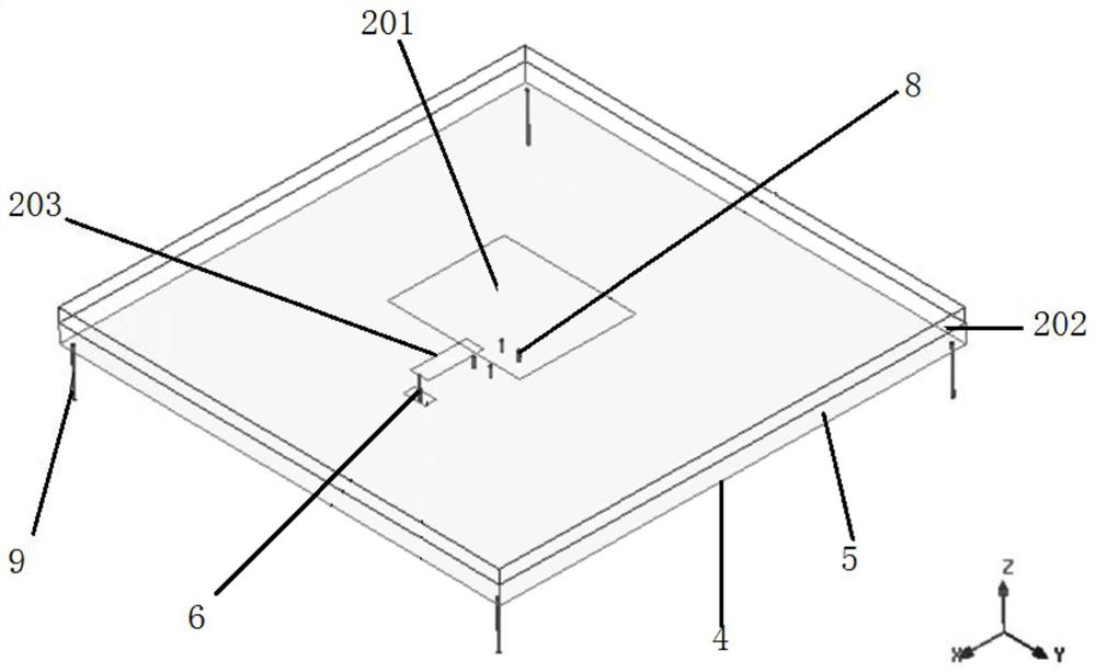
[0036] see Figure 2-Figure 10 This embodiment also proposes a millimeter-wave packaged antenna based on a fan-out packaging process, including an external substrate pad 3, a chip packaging layer 1, a reflective metal layer 4, a first passivation layer 5 and The antenna radiation structure 2, and at least one first signal via hole 6 and at least one second signal via hole 7; the first signal via hole 6 is arranged through the first passivation layer 5 and the reflective metal layer 4, and the second One end of a signal through hole 6 is connected to the antenna radiation structure 2, and the other end is connected to the chip packaging layer 1, and the antenna radiation structure 2 performs signal transmission with the chip packaging layer 1 through the first signal through hole 6; Two signal vias 7 are disposed in the chip packaging layer 1 , and the chip packaging layer 1 performs signal transmission with the external substrate pad 3 through the second signal vias 7 .
[00...
Embodiment 3
[0049] This embodiment proposes a millimeter-wave packaged antenna based on a fan-out packaging process, wherein the millimeter-wave bare chip 101 includes a chip floor 1011, and the millimeter-wave packaged antenna further includes at least one third signal via 8 and at least one first Four signal vias 9; the reflective metal layer 4 communicates with the chip floor 1011 through the third signal via 8; the reflective metal layer 4 communicates with the external substrate pad through the fourth signal via 9 3 connected.
[0050] In a specific implementation process, the reflective metal layer 4 communicates with the chip floor 1011 through the third signal via 8; the reflective metal layer 4 communicates with the external substrate pad through the fourth signal via 9 3 connected to realize the chip floor 1011, the reflective metal layer 4 and the reference potential point of the external substrate pad 3 are connected together, which can form a common ground with the floor of t...
PUM
 Abstract
Description
Claims
Application Information
 - R&D
- Intellectual Property
- Life Sciences
- Materials
- Tech Scout
- Unparalleled Data Quality
- Higher Quality Content
- 60% Fewer Hallucinations
Browse by: Latest US Patents, China's latest patents, Technical Efficacy Thesaurus, Application Domain, Technology Topic, Popular Technical Reports.
© 2025 PatSnap. All rights reserved.Legal|Privacy policy|Modern Slavery Act Transparency Statement|Sitemap|About US| Contact US: help@patsnap.com