Composite memory structure

A memory and composite technology, applied in the direction of semiconductor devices, electric solid devices, electrical components, etc., can solve the problem of low bit density of memory components, and achieve the effect of increasing bit density and improving reliability

Pending Publication Date: 2022-03-04
POWERCHIP SEMICON MFG CORP
View PDF0 Cites 0 Cited by
  • Summary
  • Abstract
  • Description
  • Claims
  • Application Information

AI Technical Summary

Problems solved by technology

However, since the transistors occupy a large chip area, the bit density of the memory device is reduced.

Method used


Image

  • Composite memory structure
  • Composite memory structure
  • Composite memory structure

Examples


Embodiment Construction

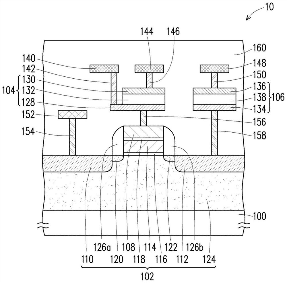
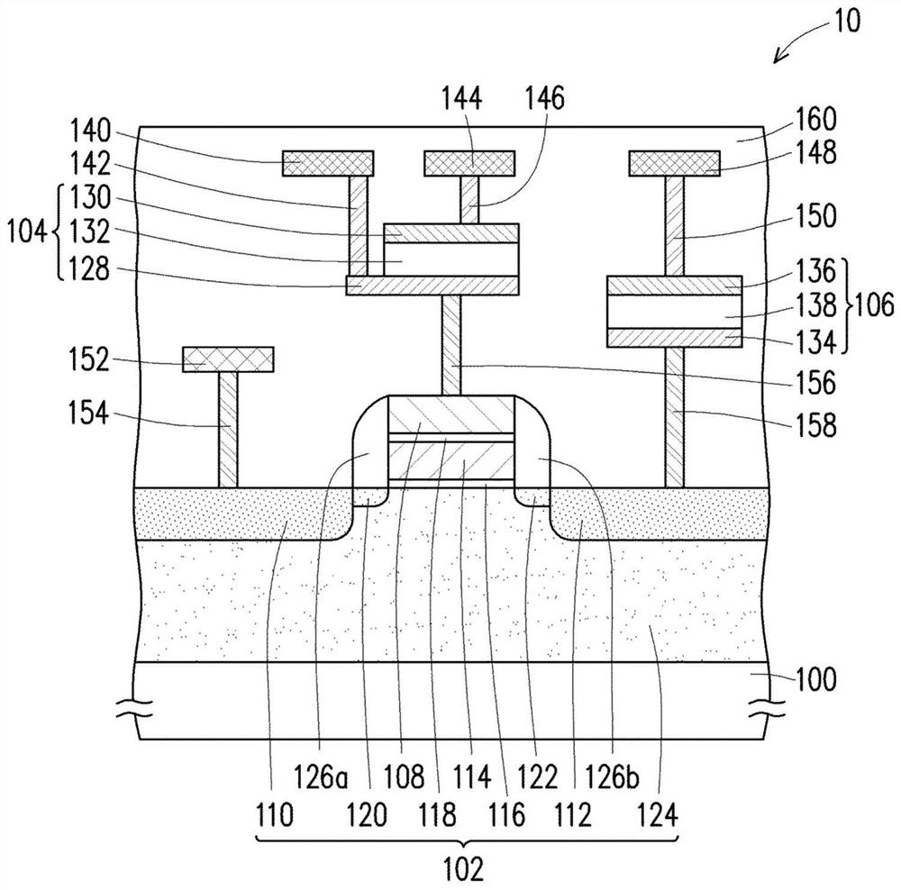
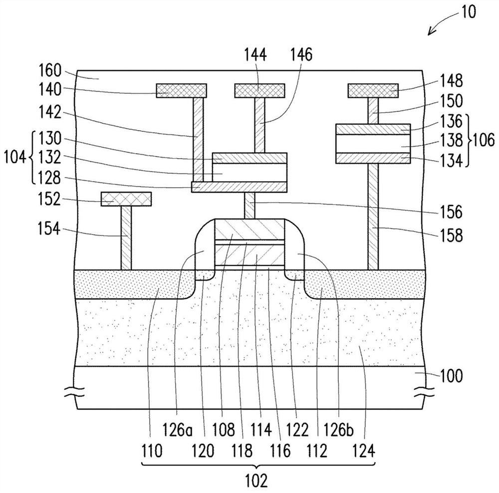
[0049] figure 1 It is a cross-sectional view of a composite memory structure according to an embodiment of the present invention. figure 2 is a cross-sectional view of a composite memory structure according to another embodiment of the present invention. image 3 is a cross-sectional view of a composite memory structure according to another embodiment of the present invention.

[0050] Please refer to figure 1 The composite memory structure 10 includes a substrate 100 , a flash memory 102 , a resistive random access memory 104 and a resistive random access memory 106 . The flash memory 102 is located on the substrate 100 . The substrate 100 may be a semiconductor substrate, such as a silicon substrate. In addition, in the circuit, the flash memory 102 , the RRAM 104 and the RRAM 106 can be three resistors connected in series. In some embodiments, the flash memory 102 , the RRAM 104 and the RRAM 106 may have the same resistance value.

[0051] The flash memory 102 includ...


PUM


Abstract

The invention discloses a composite memory structure. The composite memory structure comprises a substrate, a flash memory, a first resistive random access memory and a second resistive random access memory, the flash memory is located on the substrate. The flash memory comprises a grid electrode, a first doped region and a second doped region. The gate is on the substrate. The first doped region is located in the substrate at one side of the gate. The second doped region is located in the substrate on the other side of the gate. The first resistive random access memory is electrically connected to one of the gate, the first doped region and the second doped region. The second resistive random access memory is electrically connected to the other one of the gate, the first doped region and the second doped region.

Description

technical field [0001] The present invention relates to a semiconductor structure, and more particularly to a hybrid memory structure. Background technique [0002] Since resistive random access memory (RRAM) has a problem of leakage current, the resistive random access memory (RRAM) is electrically connected to a transistor to solve the problem of leakage current. However, since the transistor occupies a large chip area, the bit density of the memory device is reduced. Contents of the invention [0003] The invention provides a compound memory structure, which can improve the reliability and bit density of memory elements. [0004] The invention proposes a composite memory structure, including a substrate, a flash memory, a first resistive random access memory and a second resistive random access memory. Flash memory is on the substrate. The flash memory includes a gate, a first doped region and a second doped region. The gate is on the substrate. The first doped reg...

Claims


Application Information

Patent Timeline
Patent Type & Authority Applications(China)
IPC IPC(8): H01L27/24H01L27/11517H01L27/11563
CPCH10B63/00H10B41/00H10B43/00H01L29/40117H01L29/40114H10B63/30H10B63/80H10N70/20H10N70/826H10N70/8833H10B41/40H10B43/40H01L25/0652H10B41/60
Inventor 马晨亮王子嵩
Owner POWERCHIP SEMICON MFG CORP
Why Eureka
Try Eureka