Supercharge Your Innovation With Domain-Expert AI Agents!

Packaging colloid, high-brightness mini-LED structure and manufacturing process of mini-LED structure

A mini-led, encapsulating colloid technology, applied in the direction of electric solid devices, semiconductor devices, electrical components, etc., can solve the problems of light energy loss, brightness decline, etc., to achieve the effect of high brightness, not easy to damage, and convenient manufacturing process

Pending Publication Date: 2022-03-08
深圳市兆纪光电有限公司
View PDF4 Cites 1 Cited by
  • Summary
  • Abstract
  • Description
  • Claims
  • Application Information

AI Technical Summary

Problems solved by technology

[0004] In view of the related technologies mentioned above, the inventor believes that although the use of three-layer diffusion film makes the point light source of the light-emitting chip tend to become a planar light source, it also causes the loss of light energy, thereby reducing the brightness

Method used


Image

  • Packaging colloid, high-brightness mini-LED structure and manufacturing process of mini-LED structure
  • Packaging colloid, high-brightness mini-LED structure and manufacturing process of mini-LED structure
  • Packaging colloid, high-brightness mini-LED structure and manufacturing process of mini-LED structure

Examples


Embodiment Construction

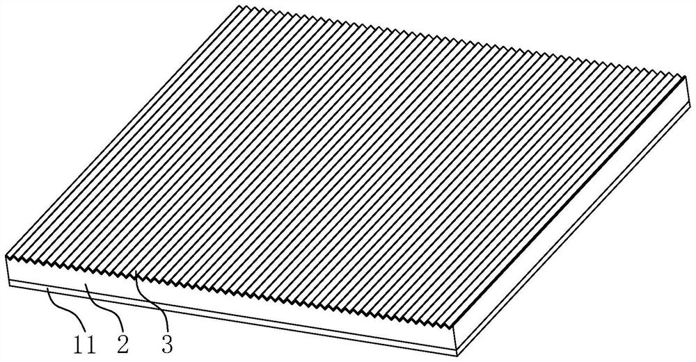
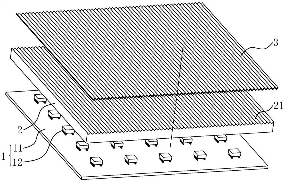
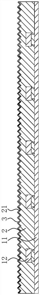
[0035] The following is attached Figure 1-3 The application is described in further detail.

[0036] The embodiment of the present application discloses an encapsulation colloid.

[0037] refer to figure 1 and figure 2 , an encapsulant for encapsulating light-emitting chips on a substrate 11, including an encapsulant 2 made of UV glue, one side of the encapsulant 2 is provided with several V-shaped grooves 21, and two adjacent V-shaped grooves The groove walls of 21 are in contact, the notch opening angle of V-shaped groove 21 is 20-105°, the groove bottom distance between two adjacent V-shaped grooves 21 is 0.05-0.2mm, and the depth of V-shaped groove 21 is 0.05-0.2mm. mm.

[0038] When in use, the V-shaped groove 21 on the encapsulant 2 refracts and diverges the light of the mini-LED, so that the point light source of the mini-LED tends to be a planar light source, so that the point light source of the light-emitting chip does not need to diffuse through multiple layer...


PUM


Abstract

The invention relates to a packaging colloid, and relates to the field of mini-LEDs, the packaging colloid comprises a packaging colloid made of a high light transmittance material, the surface of the packaging colloid is provided with a plurality of V-shaped grooves, and the groove walls of two adjacent V-shaped grooves are in contact. The invention further relates to a high-brightness mini-LED structure which comprises a carrier plate and the packaging colloid, the carrier plate comprises a substrate and a light-emitting chip, the light-emitting chip is attached to one side of the substrate, the packaging colloid is located on the side, close to the light-emitting chip, of the substrate, the light-emitting chip is packaged on the substrate, and the light-emitting chip is sealed in the packaging colloid. And a layer of diffusion film is attached to the groove wall of the V-shaped groove. The invention further relates to a manufacturing process of the high-brightness mini-LED structure. The method has the effect of improving the brightness of the mini-LED.

Description

technical field [0001] The present application relates to the field of mini-LEDs, in particular to an encapsulation compound, a high-brightness mini-LED structure and a manufacturing process of the mini-LED structure. Background technique [0002] With the rapid development of mini-LED display technology, mini-LED display products have a wider range of applications, and are used in monitoring and command, high-end theaters, and advertising display. [0003] At present, the most commonly used mini-LED display structure includes a substrate, a light-emitting chip, and an encapsulant. The light-emitting chip is mounted on one side of the substrate. Located in the encapsulation colloid, the side of the encapsulation colloid away from the substrate is covered with a diffusion film, and the diffusion film is provided with three layers. When in use, the point light source on the light-emitting chip emits light, and the light is diffused through the three-layer diffusion film, so t...

Claims


Application Information

Patent Timeline
Patent Type & Authority Applications(China)
IPC IPC(8): H01L33/54H01L33/56H01L25/075
CPCH01L33/54H01L33/56H01L25/0753H01L2933/005
Inventor 李思升吴王坤张利刚
Owner 深圳市兆纪光电有限公司
Features
  • R&D
  • Intellectual Property
  • Life Sciences
  • Materials
  • Tech Scout
  • Unparalleled Data Quality
  • Higher Quality Content
  • 60% Fewer Hallucinations
Learn More