Method for improving manufacturing yield of LED chip

A LED chip and yield technology, which is applied in the direction of electrical components, circuits, semiconductor devices, etc., can solve problems such as flushing water and two-fluid cleaning machines, physical damage to LED chips, and abnormal surface pollution, etc., to improve product quality. The effect of appearance yield, realization of preparation and process operation is simple

Active Publication Date: 2021-03-05
SHANDONG INSPUR HUAGUANG OPTOELECTRONICS
View PDF6 Cites 2 Cited by
  • Summary
  • Abstract
  • Description
  • Claims
  • Application Information

AI Technical Summary

Problems solved by technology

GaAs-based LED wafers are generally cut with a diamond knife. During the saw blade cutting process, the diamond knife will be in direct contact with the ITO film, which will cause serious physical damage to the LED wafer during the cutting process, especially in the cutting aisle. Edges are prone to edge chipping, cracks, corner chipping, oblique cracks, etc.
At the same time, the debris accompanying the cutting will be adsorbed to the surface of the electrode, resulting in abnormal surface contamination. It is difficult to remove by flushing water and two-fluid cleaning machine during the cutting process, which greatly affects the cutting yield.

Method used


Image

  • Method for improving manufacturing yield of LED chip

Examples


Embodiment 1

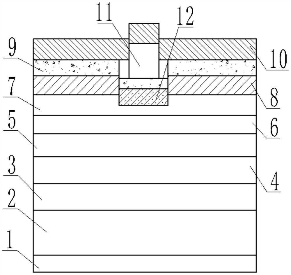
[0054] S1: Take GaAs substrate 2, and grow GaAs buffer layer 3, n-AlGaInP confinement layer 4, multi-quantum well active layer 5, p-AlGaInP confinement layer 6, first highly doped p-GaP Window layer 7 and the second highly doped p-GaP window layer 8 to obtain wafer epitaxial layer;

[0055] S2: Take the wafer after the growth of the epitaxial layer is completed, make a photoresist mask pattern on the second highly doped p-GaP window layer 8, etch to form an exposed area, and the exposed area runs through the second highly doped p-GaP window layer 8, and the bottom end of the exposed area is located in the middle of the first highly doped p-GaP window layer 7; then an oxide film 12 is deposited on the exposed area, and the oxide is TiO 2 ;

[0056] S3: Take the wafer after the evaporation treatment of the oxide film 12, and evaporate the ITO film 9 on the epitaxial layer of the wafer, and the ITO film 9 covers the entire surface of the epitaxial layer; the growth temperature o...

Embodiment 2

[0064] S1: Take GaAs substrate 2, and grow GaAs buffer layer 3, n-AlGaInP confinement layer 4, multi-quantum well active layer 5, p-AlGaInP confinement layer 6, first highly doped p-GaP Window layer 7 and the second highly doped p-GaP window layer 8 to obtain wafer epitaxial layer;

[0065] S2: Take the wafer after the growth of the epitaxial layer is completed, make a photoresist mask pattern on the second highly doped p-GaP window layer 8, etch to form an exposed area, and the exposed area runs through the second highly doped p-GaP window Layer 8, and the bottom end of the exposed area is located in the middle of the first highly doped p-GaP window layer 7; then an oxide film 12 is deposited on the exposed area, and the oxide is ZnO;

[0066] S3: Take the wafer after the evaporation treatment of the oxide film 12, and evaporate the ITO film 9 on the epitaxial layer of the wafer, and the ITO film 9 covers the entire surface of the epitaxial layer; the growth temperature of th...

Embodiment 3

[0074] S1: Take GaAs substrate 2, and grow GaAs buffer layer 3, n-AlGaInP confinement layer 4, multi-quantum well active layer 5, p-AlGaInP confinement layer 6, first highly doped p-GaP Window layer 7 and the second highly doped p-GaP window layer 8 to obtain wafer epitaxial layer;

[0075] S2: Take the wafer after the growth of the epitaxial layer is completed, make a photoresist mask pattern on the second highly doped p-GaP window layer 8, etch to form an exposed area, and the exposed area runs through the second highly doped p-GaP window Layer 8, and the bottom end of the exposed area is located in the middle of the first highly doped p-GaP window layer 7; then an oxide film 12 is deposited on the exposed area; the oxide is Al 2 o 3 ;

[0076] S3: Take the wafer after the evaporation treatment of the oxide film 12, and evaporate the ITO film 9 on the epitaxial layer of the wafer, and the ITO film 9 covers the entire surface of the epitaxial layer; the growth temperature o...


PUM


Abstract

The invention discloses a method for improving the manufacturing yield of an LED chip. The method comprises the steps: firstly carrying out the growth of a wafer epitaxial layer, then carrying out thecorrosion of a second highly-doped pGaP window layer to form an exposed region, and then depositing an oxide film; and then evaporating an ITO film on the surface of the epitaxial layer, continuouslymanufacturing a P-surface electrode and an N-surface electrode, finally evaporating a protective film on the surface of the P-surface electrode, then performing cutting, ultrasonically removing the protective film through hot water after cutting, and finally cleaning and expanding the film of the chip to form independent single core particles. According to the method, preparation of the LED chipis effectively achieved, the light-emitting effect of the chip is improved, MgF2 / CaF2 films alternately grow on the surface of the wafer, the light-emitting surface is smooth, the problems that in thecutting process, a diamond knife makes direct contact with an ITO film, and corner breakage, cracks and the like are likely to be generated are solved, the product quality and reliability are greatlyimproved, chippings and water stain and dirt residues in the cutting process are avoided, the product appearance yield is increased, and high practicability is achieved.

Description

technical field [0001] The invention relates to the technical field of semiconductor processing, in particular to a method for improving the yield rate of LED chip manufacturing. Background technique [0002] Traditional incandescent lamps consume a lot of energy and have a short lifespan. Today, when global resources are in short supply, their production has been gradually banned by governments of various countries. The replacement products are electronic energy-saving lamps. Although electronic energy-saving lamps improve energy-saving effects, they pollute the environment due to the use of many heavy metal elements, which is contrary to the general trend of environmental protection. With the rapid development of LED technology, LED lighting has gradually become the best choice for new green lighting. LED is a semiconductor device that uses carrier recombination to emit light. LED chips have many advantages such as low power consumption, pure chromaticity, long life, smal...

Claims


Application Information

Patent Timeline
IPC IPC(8): H01L33/14H01L33/44H01L33/00
CPCH01L33/0062H01L33/14H01L33/145H01L33/44H01L2933/0025
Inventor 王梦雪吴向龙闫宝华王成新徐现刚
Owner SHANDONG INSPUR HUAGUANG OPTOELECTRONICS
Why Eureka
Try Eureka