
Communication lumped parameter circulator based on MEMS technology and manufacturing method thereof

A technology of lumped parameters and production methods, applied in waveguide devices, electrical components, circuits, etc., can solve problems that cannot meet the development of microstrip circulators, improve production efficiency and product consistency, reduce process difficulty, prevent damage

Active Publication Date: 2022-03-08
SOUTHWEST INST OF APPLIED MAGNETICS
View PDF7 Cites 6 Cited by
  • Summary
  • Abstract
  • Description
  • Claims
  • Application Information

AI Technical Summary

Problems solved by technology

The traditional processing technology can no longer meet the development of microstrip circulators, so silicon-based microstrip circulators based on MEMS technology came into being
[0005] In a general sense, silicon-based microstrip circulators based on MEMS technology are mainly made by combining two upper and lower silicon substrates. It is realized by metal bonding of silicon wafers, but this method is mainly used to make circulators with microstrip / stripline structure, because the miniaturization of lumped parameter circulators requires multi-layer circuits to be built into woven bag structures, generally two pieces The combination of silicon wafers cannot meet this requirement (design effect), so it needs to be manufactured in the form of multi-layer circuits, that is, there is an urgent need in this field for a method of manufacturing lumped parameter circulators based on MEMS technology to solve the above problems

Method used


Image

  • Communication lumped parameter circulator based on MEMS technology and manufacturing method thereof
  • Communication lumped parameter circulator based on MEMS technology and manufacturing method thereof
  • Communication lumped parameter circulator based on MEMS technology and manufacturing method thereof

Examples


Embodiment 1

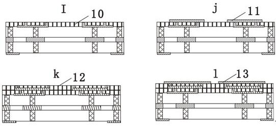
[0049] A lumped parameter circulator for communication based on MEMS technology, see Figure 7 , its main structure includes a silicon master substrate 1, a silicon sub-substrate 2 is arranged below the silicon master substrate 1, and two layers of polyimide films are arranged above the silicon master substrate 1, respectively A layer of polyimide 10 and a second layer of polyimide 12; circuit patterns are made on the upper surface and the lower surface of the silicon master substrate 1 and the silicon sub-substrate 2, and the silicon master substrate 1 It is interconnected with the silicon sub-substrate 2 through metal vias and bonding; the polyimide film on each layer is also made with a circuit pattern, and is interconnected with the circuit of the lower layer through the metallized vias on the polyimide film;

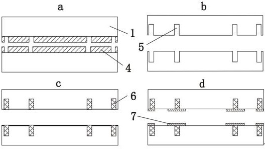
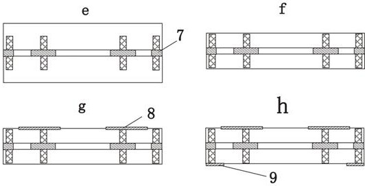
[0050] The manufacture method of above-mentioned circulator, see Figure 1-4 , including the following steps:

[0051] (1) Use a double-sided polished high-resista...


PUM

PropertyMeasurementUnit
electrical resistivityaaaaaaaaaa
thicknessaaaaaaaaaa
electrical resistivityaaaaaaaaaa

Abstract

The invention discloses a lumped parameter circulator for communication based on an MEMS technology and a manufacturing method of the lumped parameter circulator, and belongs to the technical field of microwave components, the lumped parameter circulator comprises a silicon main substrate, a silicon auxiliary substrate is arranged below the silicon main substrate, and at least two layers of polyimide films are arranged above the silicon main substrate; circuit patterns are manufactured on the upper surfaces and the lower surfaces of the main silicon substrate and the auxiliary silicon substrate, and the main silicon substrate and the auxiliary silicon substrate are interconnected in a metal via hole and bonding mode; each layer of polyimide film is also provided with a circuit pattern, and is interconnected with a circuit at the lower layer through a metalized through hole in the polyimide film; the lumped parameter microstrip circulator manufactured by using the MEMS process technology has the size as small as 3 * 3mm, has the advantages of mature process, high speed, low cost, high efficiency, good consistency and the like, is suitable for mass production, can effectively reduce the sizes of ferrite and devices, and lays a process foundation for smaller devices such as 2 * 2mm and 1 * 1mm.

Description

technical field [0001] The invention relates to the technical field of microwave components, in particular to a lumped parameter circulator for communication based on MEMS technology and a manufacturing method thereof. Background technique [0002] The circulator is an important basic device in microwave engineering. It is widely used in various civil and military equipment such as civil communication, microwave measurement, radar, communication, electronic countermeasures, and aerospace. It is mainly used to realize the antenna in the equipment. Sending and receiving sharing, inter-level isolation and other issues. It usually works in the S-band and below frequency bands, and is widely used in 4G and 5G communication base stations. Lumped microstrip circulators are very important in contemporary communication systems due to their small size, light weight, and easy integration. status. [0003] At present, the main production method of the lumped parameter circulator is to...

Claims


Application Information

Patent Timeline
Patent Type & Authority Applications(China)
IPC IPC(8): H01P1/383H01P11/00
CPCH01P1/383H01P11/00
Inventor 李晓宇冯楠轩王梦佳彭根斋兰洋胡艺缤张志红
Owner SOUTHWEST INST OF APPLIED MAGNETICS
Learn More