Clock circuit and memory

A clock circuit and clock technology, applied in static memory, digital memory information, logic circuits, etc., can solve the problem of mismatch between the system clock signal and the data strobe clock signal, and achieve synchronization and handshake functions. small change effect

Pending Publication Date: 2022-03-15
CHANGXIN MEMORY TECH INC
View PDF0 Cites 2 Cited by
  • Summary
  • Abstract
  • Description
  • Claims
  • Application Information

AI Technical Summary

Problems solved by technology

[0005] The technical problem solved by the embodiments of the present invention is to provide a clock circuit and memory to solve the problem of mismatch between the system clock signal and the data strobe clock signal

Method used


Image

  • Clock circuit and memory
  • Clock circuit and memory
  • Clock circuit and memory

Examples


Embodiment Construction

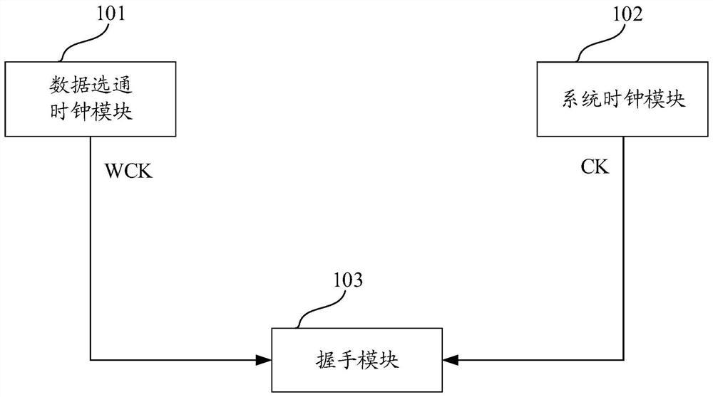
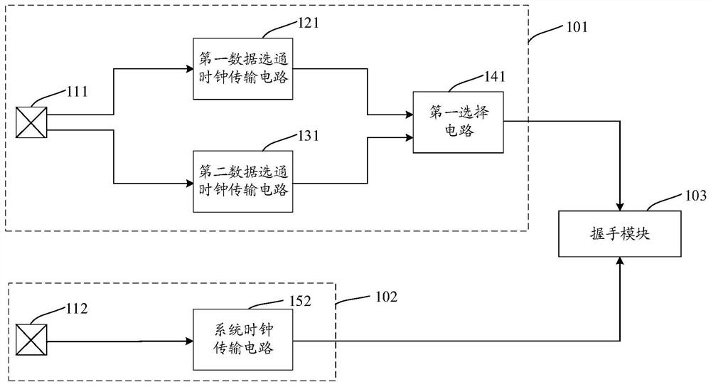
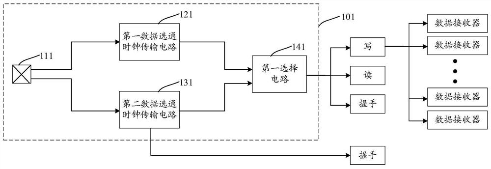
[0035] In order to alleviate the timing constraints of reading and writing of the memory, a WCK clock signal, that is, a data strobe clock signal, is introduced into the memory. In order to meet different performance requirements, the data transmission rate of the same memory can be fast or slow, and the transmission rate of the corresponding WCK clock signal can be a transmission rate exceeding a preset value, or a transmission rate lower than a preset value. For example, when the data transmission rate exceeds 3200Mbps, a current mode logic (CML, Current ModeLogic) frequency divider can be introduced to reduce the interference on the WCK clock signal; when the data transmission rate is lower than 3200Mbps, a CMOS frequency divider can be used to Maximum power saving.

[0036] That is to say, if the transmission rate of the WCK clock signal in the memory is different, the WCK clock signal is transmitted through different transmission paths. There is also a CK clock signal (s...


PUM


Abstract

The embodiment of the invention provides a clock circuit and a memory, and the clock circuit comprises a data gating clock module which is used for receiving a data gating clock signal and transmitting the data gating clock signal, and the data gating clock signal is used for controlling the receiving and/or sending of a data signal; the system clock module is used for receiving a system clock signal and transmitting the system clock signal, and the system clock signal is used for controlling receiving of a command signal; wherein the system clock module comprises at least two first signal transmission paths, and is configured to adopt different first signal transmission paths to transmit the system clock signal according to different receiving and/or sending rates of the data signal.

Description

technical field [0001] Embodiments of the present invention relate to the technical field of semiconductors, and in particular to a clock circuit and a memory. Background technique [0002] Dynamic Random Access Memory (Dynamic Random Access Memory, DRAM) is a semiconductor storage device commonly used in computers, and is composed of many repeated storage units. Each memory cell usually includes a capacitor and a transistor. The gate of the transistor is connected to the word line, the drain is connected to the bit line, and the source is connected to the capacitor. The voltage signal on the word line can control the opening or closing of the transistor, and then through the bit line Read the data information stored in the capacitor, or write the data information into the capacitor through the bit line for storage. [0003] DRAM can be divided into Double Data Rate (DDR) DRAM, GDDR (Graphics Double Data Rate) DRAM, and Low Power Double Data Rate (LPDDR) DRAM. As DRAM is a...

Claims


Application Information

Patent Timeline
Patent Type & Authority Applications(China)
IPC IPC(8): G11C11/406G11C11/4076
CPCG11C11/406G11C11/4076G11C7/222G11C7/1093H03K19/09432
Inventor 林峰
Owner CHANGXIN MEMORY TECH INC
Why Eureka
Try Eureka