

Method and system for reducing circuit absorption or emission power of printed circuit board
A printed circuit board, transmitting power technology, applied in the direction of printed circuit, printed circuit manufacturing, printed circuit components, etc., can solve the problems of poor anti-interference performance of the circuit board, reduce the stability of the circuit board, etc., to improve the anti-electromagnetic interference the effect of the ability
- Summary
- Abstract
- Description
- Claims
- Application Information
AI Technical Summary
Problems solved by technology
Method used
Image

Examples
Embodiment Construction
[0042] Embodiments of the present invention are described in detail below, examples of which are shown in the drawings, wherein the same or similar reference numerals designate the same or similar elements or elements having the same or similar functions throughout. The embodiments described below by referring to the figures are exemplary and are intended to explain the present invention and should not be construed as limiting the present invention.
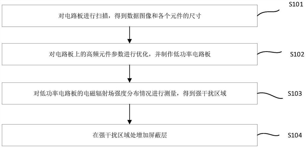
[0043] see Figure 1 to Figure 7 , In a first aspect, the present invention provides a method for reducing the absorption or emission power of a printed circuit board circuit, comprising:
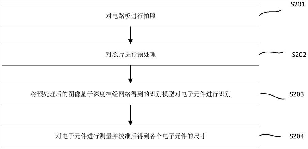
[0044] S101 scans the circuit board to obtain the data image and the size of each component;
[0045] The specific steps are:
[0046] S201 taking pictures of the circuit board;
[0047] Use a high-precision camera to take pictures of the circuit board, preferably in the forward direction to reduce the distortion generated when taking pictu...
PUM
 Abstract
Description
Claims
Application Information