

Blue-ray LED driving system with adjustable brightness
A LED drive and blue light technology, applied in the field of electronic energy saving, can solve the problems of poor anti-electromagnetic interference ability, unstable driving, poor brightness adjustment accuracy, etc., to improve load capacity, improve anti-electromagnetic interference ability, and ensure stability Effect
- Summary
- Abstract
- Description
- Claims
- Application Information
AI Technical Summary
Problems solved by technology
Method used
Image

Examples
Embodiment
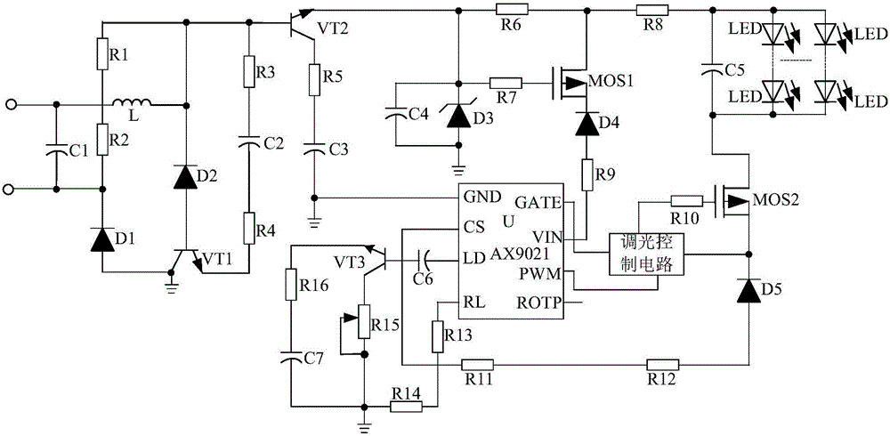
[0022] Such as figure 1 As shown, the present invention is mainly composed of a control chip U, a dimming control circuit, a reference correction circuit, a slope compensation circuit, and a logic buffer circuit. The reference correction circuit is composed of triode VT1, triode VT2, resistor R1, resistor R2, resistor R3, resistor R4, resistor R5, polar capacitor C1, polar capacitor C2, polar capacitor C3, inductor L, diode D1, and diode D2 composition.
[0023] When connected, the P pole of the diode D2 is connected to the base of the transistor VT1, and the N pole is connected to the base of the transistor VT2. The P pole of the diode D1 is connected to the collector of the triode VT1, and the N pole is connected to the base of the triode VT2 through the resistor R2 and the resistor R1 in sequence. The anode of the polarity capacitor C1 is connected to the base of the transistor VT2 after passing through the inductor L, and the cathode is connected to the N pole of the dio...
PUM
 Abstract
Description
Claims
Application Information