System and method for testing mark size of photomask substrate
A testing system and testing method technology, applied in optics, measuring devices, using optical devices, etc., can solve problems such as high equipment cost, scratches, and scrapped substrates, and achieve the effect of low measurement cost and scratch avoidance
- Summary
- Abstract
- Description
- Claims
- Application Information
AI Technical Summary
Problems solved by technology
Method used
Image
Examples
Embodiment Construction
[0031] In order to better understand the present invention, the present invention will be further described below in conjunction with the accompanying drawings and specific embodiments.
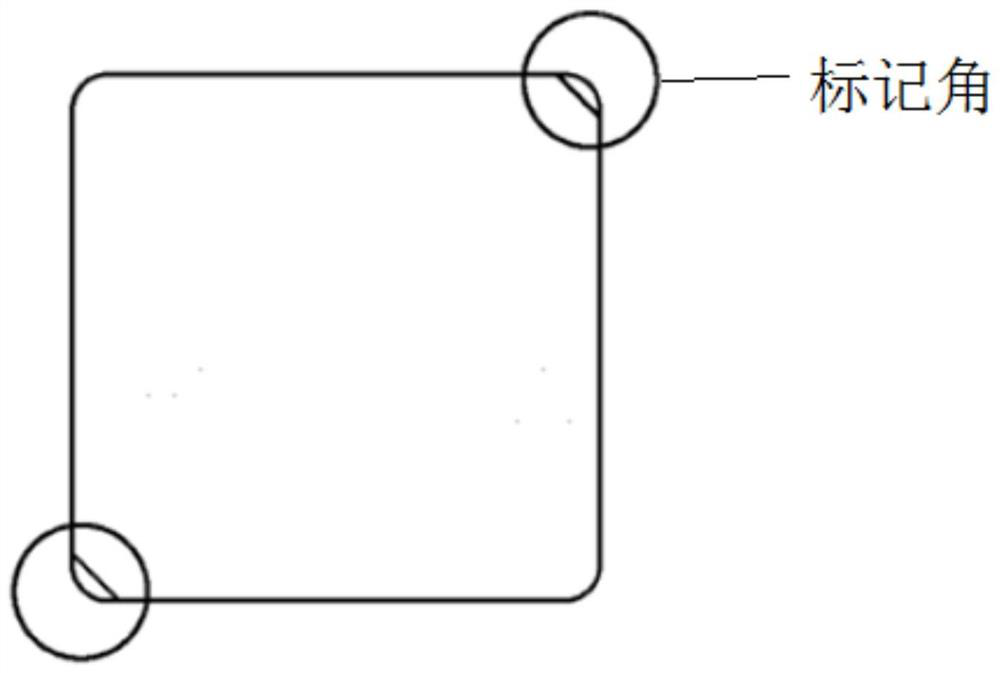
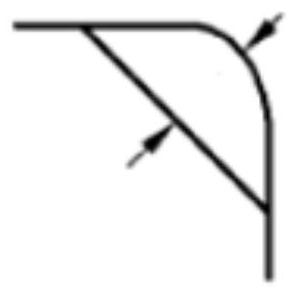
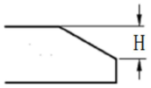
[0032] Such as Figure 1~2 Shown is a photomask substrate, its four corners are chamfered corners, and the two obliquely opposite chamfered corners are marked corners, and the upper surface of the marked corners is inclined downward to form a slope. The height of the slope is also the depth of the mark, which is to be Tested mark size H, such as image 3 shown. In this embodiment, the marking angle is characterized by: it is located at the edge of the photomask substrate; and its shape is an arc-shaped area.
[0033] Such as Figure 4 A kind of photomask substrate marking size testing system shown, comprises three-dimensional mobile platform 2, light source 3, focusing lens 4, camera 5, computer 6 and controller 7; The middle part of described three-dimensional mobile platform 3 is provide...
PUM
 Abstract
Description
Claims
Application Information
 - R&D Engineer
- R&D Manager
- IP Professional
- Industry Leading Data Capabilities
- Powerful AI technology
- Patent DNA Extraction
Browse by: Latest US Patents, China's latest patents, Technical Efficacy Thesaurus, Application Domain, Technology Topic, Popular Technical Reports.
© 2024 PatSnap. All rights reserved.Legal|Privacy policy|Modern Slavery Act Transparency Statement|Sitemap|About US| Contact US: help@patsnap.com


