Formation method of semiconductor structure
A semiconductor and gate structure technology, which is applied in the field of semiconductor structure formation, can solve the problems that the performance of semiconductor structures needs to be further improved, and achieve the effect of small performance
- Summary
- Abstract
- Description
- Claims
- Application Information
AI Technical Summary
Problems solved by technology
Method used
Image

Examples
Embodiment Construction
[0031] As mentioned in the background, the manufacturing process of the local interconnect structure in the prior art needs to be improved, and the performance of the formed semiconductor structure needs to be further improved. Now analyze and illustrate in conjunction with specific embodiment.
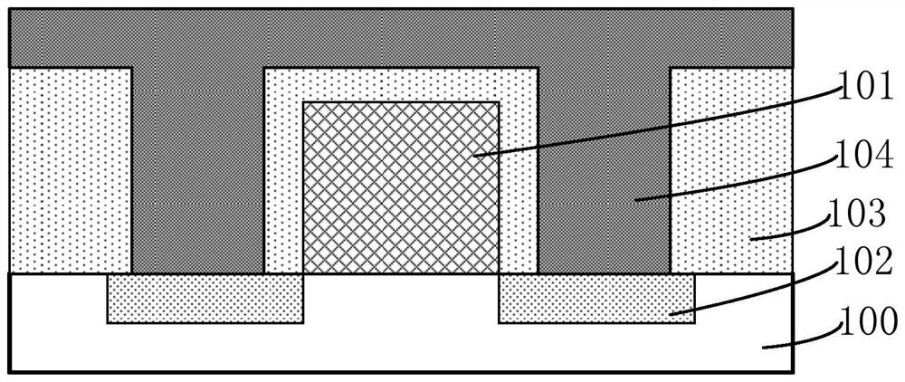
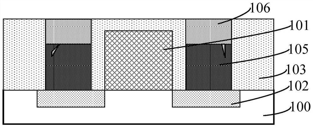
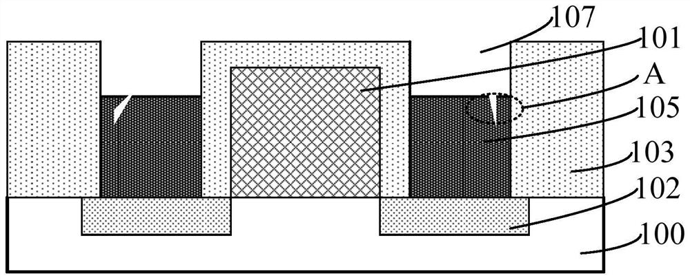
[0032] Figure 1 to Figure 3 It is a schematic cross-sectional structure diagram of the formation process of the semiconductor structure in an embodiment.
[0033] Please refer to figure 1 , providing a substrate 100; forming a gate structure 101 on the substrate 100; forming a source-drain doped region 102 in the substrate on both sides of the gate structure 101; forming a first dielectric layer 103 on the substrate; An opening (not shown) is formed in the dielectric layer 103, and the opening exposes the surface of the source-drain doped region 102; a conductive material layer 104 is formed in the opening and on the first dielectric layer 103; annealing is performed on the conduct...
PUM
 Abstract
Description
Claims
Application Information
 - R&D
- Intellectual Property
- Life Sciences
- Materials
- Tech Scout
- Unparalleled Data Quality
- Higher Quality Content
- 60% Fewer Hallucinations
Browse by: Latest US Patents, China's latest patents, Technical Efficacy Thesaurus, Application Domain, Technology Topic, Popular Technical Reports.
© 2025 PatSnap. All rights reserved.Legal|Privacy policy|Modern Slavery Act Transparency Statement|Sitemap|About US| Contact US: help@patsnap.com