

Fast flushing and quick discharge tank for integrated circulation cooling and cleaning of semiconductor wafers
A cyclic cooling, semiconductor technology, applied in the field of semiconductor wafer processing, fast flushing and fast slotting, can solve the problems of surface residue, damage, uneven cleaning, etc., to achieve the effect of cleaning the wafer thoroughly and avoiding damage
- Summary
- Abstract
- Description
- Claims
- Application Information
AI Technical Summary
Problems solved by technology
Method used
Image

Examples
Embodiment Construction
[0039] Embodiments of the present invention provides a fast-flush fast-loading groove for semiconductor wafer integrated circulating cooling cleaning.
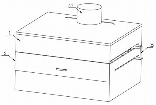
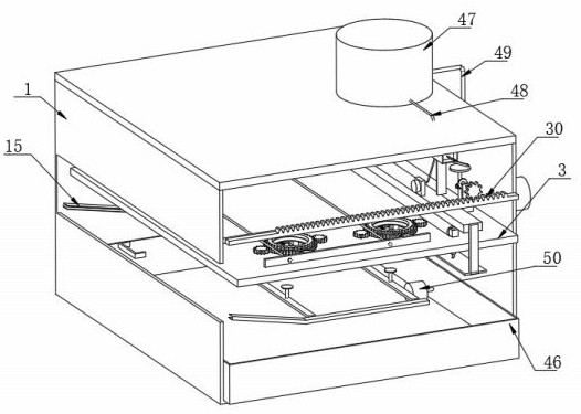
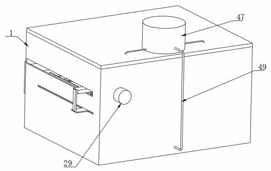
[0040] See Figure 1 、 Figure 2 、 Figure 3 、 Figure 4 、 Figure 5 、 Figure 6 、 Figure 7 、 Figure 8 and Figure 15, including cleaning tank 1, cleaning tank 1 outer rotation connected to the cover plate 2, cleaning tank 1 on both sides of the inner wall are fixed to connect to the sliding frame 52, between the two sliding rack 52 is provided with a fixed plate 3 and the fixed plate 3 sliding connection, the fixed plate 3 top is opened with multiple through grooves 4, the fixed plate 3 is equipped with a placement groove 56, multiple placement grooves 56 are distributed around multiple grooves 4 rings and communicate with the groove 4, the fixed plate 3 is equipped with multiple rings of gear 5, multiple rings of gear 5 correspond to multiple grooves 4 one by one, Multiple rings of gear 5 are connected to the fixed plate 3 by mean...
PUM
 Abstract
Description
Claims
Application Information