Novel OLED pixel structure and arrangement method
A pixel structure, a new technology, applied in the direction of electrical components, electrical solid devices, circuits, etc., to achieve the effects of reducing graininess, saving costs, and improving panel color cast
- Summary
- Abstract
- Description
- Claims
- Application Information
AI Technical Summary
Problems solved by technology
Method used
Image


Examples
Embodiment Construction
[0025] The following will clearly and completely describe the technical solutions in the embodiments of the present invention with reference to the accompanying drawings in the embodiments of the present invention. Obviously, the described embodiments are only some, not all, embodiments of the present invention. Based on the embodiments of the present invention, all other embodiments obtained by persons of ordinary skill in the art without making creative efforts belong to the protection scope of the present invention.
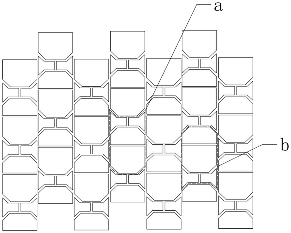
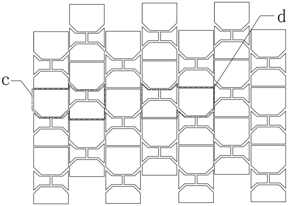
[0026] According to the human eye's perception of RGB light, green light is the most sensitive, red light is the second, and blue light is the weakest. Among OLED organic light-emitting materials, blue life is the shortest, green is second, and red is the longest. Under the premise of meeting the process conditions , increase the blue sub-pixel area as much as possible, and array it on the panel in a specific way.
[0027] The present invention provides such a...
PUM
 Abstract
Description
Claims
Application Information
 - R&D
- Intellectual Property
- Life Sciences
- Materials
- Tech Scout
- Unparalleled Data Quality
- Higher Quality Content
- 60% Fewer Hallucinations
Browse by: Latest US Patents, China's latest patents, Technical Efficacy Thesaurus, Application Domain, Technology Topic, Popular Technical Reports.
© 2025 PatSnap. All rights reserved.Legal|Privacy policy|Modern Slavery Act Transparency Statement|Sitemap|About US| Contact US: help@patsnap.com