Test method for laser chip

A test method and chip technology, applied in the direction of electronic circuit testing, measuring electricity, measuring devices, etc., can solve problems such as inconsistency and test data instability, eliminate fatigue problems, eliminate small rotational offsets, and improve stability. Effect

Pending Publication Date: 2022-04-12
STELIGHT INSTR CO LTD
View PDF0 Cites 1 Cited by
  • Summary
  • Abstract
  • Description
  • Claims
  • Application Information

AI Technical Summary

Problems solved by technology

Based on the above findings, the purpose of the present invention is to provide a test method for laser chips, which solves the problem of long-term use due to the fatigue of the probe station in the prior art. Instability and inconsistency of test data

Method used


Image

  • Test method for laser chip
  • Test method for laser chip
  • Test method for laser chip

Examples


Embodiment 1

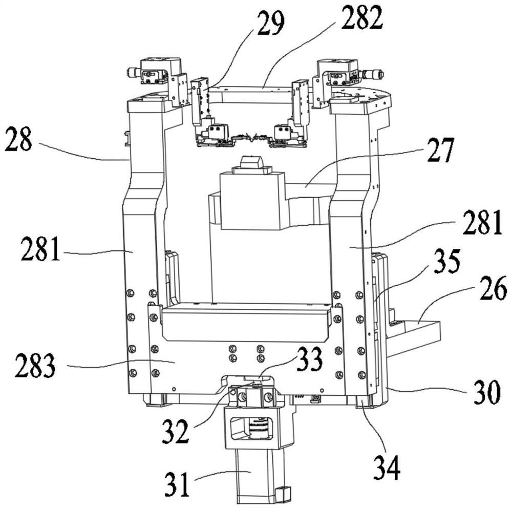
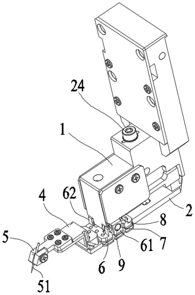
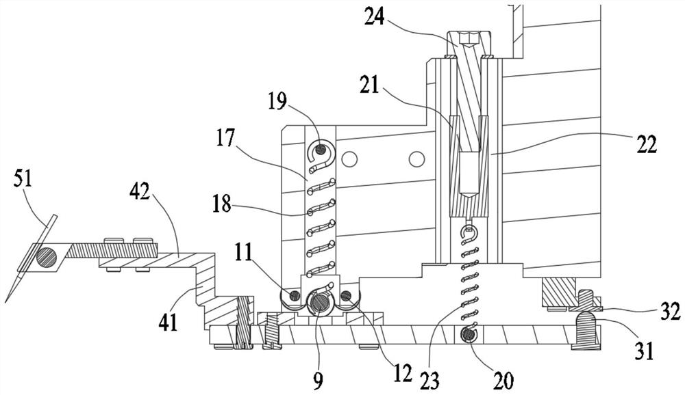
[0030]Embodiment 1: a kind of testing method that is used for laser chip, based on a testing device, described testing device comprises substrate 26, is installed on the test stand 27 of substrate 26 upper surface, is installed on the driving support 28 of substrate 26 outsides and is installed on The test probe assembly 29 on the drive bracket 28 and positioned above the test bench 27, the test probe assembly 29 includes: a body 1 connected to the drive bracket 28, a support plate 2, a probe 51 for contacting the chip to be tested and a moving point contact probe 31, a cantilever 4 is installed at one end of the support plate 2, and the moving point contact probe 31 is installed at the other end, and one side of the lower end surface of the body 1 is arranged on the upper part of the moving point contact probe 31 and corresponds to it. The static point of the contact probe 32, the end of the cantilever 4 away from the support plate 2 is fixed with a probe base 5 equipped with ...

Embodiment 2

[0040] Embodiment 2: a kind of testing method that is used for laser chip, based on a testing device, described testing device comprises substrate 26, is installed on the test platform 27 of substrate 26 upper surface, is installed on the driving support 28 of substrate 26 outsides and is installed on The test probe assembly 29 on the drive bracket 28 and positioned above the test bench 27, the test probe assembly 29 includes: a body 1 connected to the drive bracket 28, a support plate 2, a probe 51 for contacting the chip to be tested and a moving point contact probe 31, a cantilever 4 is installed at one end of the support plate 2, and the moving point contact probe 31 is installed at the other end, and one side of the lower end surface of the body 1 is arranged on the upper part of the moving point contact probe 31 and corresponds to it. The static point of the contact probe 32, the end of the cantilever 4 away from the support plate 2 is fixed with a probe base 5 equipped w...


PUM


Abstract

The invention discloses a test method for a laser chip, and the method is based on a test device which comprises a substrate, a test bench disposed on the upper surface of the substrate, a drive support disposed on the outer side of the substrate, and a test probe assembly which is disposed on the drive support and is located above the test bench. The testing probe assembly comprises a body connected with the driving support, a supporting plate, a probe used for making contact with a chip to be tested and a movable point contact probe, a cantilever is installed at one end of the supporting plate, and the movable point contact probe is installed at the other end of the supporting plate. One side of the lower end face of the body is provided with a static point contact probe which is located on the upper portion of the movable point contact probe and corresponds to the movable point contact probe. The end, away from the supporting plate, of the cantilever is fixedly provided with a probe base provided with the probe. According to the invention, the accuracy of the detection status is ensured, and the stability, repeatability, comparability and consistency of the detection data are further improved.

Description

technical field [0001] The invention relates to a testing method for a laser chip, which belongs to the technical field of chip testing. Background technique [0002] In the production and testing process of lasers in the optical communication industry, before the COC aging process, it is also necessary to conduct a photoelectric performance test of a single laser chip (Laser Diode, LD), so that the performance of the laser chip (LD) can be screened before aging, and the performance Problematic lasers are picked out in advance, thereby improving the overall yield after COC burn-in. [0003] In the testing process of a single laser chip (LD) in optical communication, the stability of the probe plays a very important role. At least it will push the position or angle of the chip to shift. Once the position and angle of the chip change, it will directly affect the stability of subsequent test indicators and test efficiency, and the pressure stability of the test probe will also...

Claims


Application Information

Patent Timeline
Patent Type & Authority Applications(China)
IPC IPC(8): G01R31/28G01R1/04G01R1/067G01R1/073
Inventor 黄建军吴永红赵山胡海洋
Owner STELIGHT INSTR CO LTD
Why Eureka
Try Eureka