Light splitting film and preparation method and system thereof
A technology for preparing a system and spectroscopic film, which is applied in the field of spectroscopic film, can solve the problems of increasing the overall thickness of the structure, uneven light distribution, and undesirable bright spots, etc., and achieve the effect of improving uniformity and luminance, improving shading, and easy thickness
- Summary
- Abstract
- Description
- Claims
- Application Information
AI Technical Summary
Problems solved by technology
Method used
Image
Examples
Embodiment 1
[0053] The present invention provides a spectroscopic film 1, such as figure 1 shown, including:
[0054] PSA layer 2;
[0055] And the raised microstructure layer 3 attached to the PSA layer 2;
[0056] The protrusions of the raised microstructure layer 3 are far away from the PSA layer;
[0057] The raised microstructure layer 3 is a hollow structure.
[0058] The raised microstructure layer 3 is Microlens, triangular pyramid, quadrangular pyramid or prism ( figure 1 The raised microstructure layer 3 only shows the Microlens structure, and it should be understood that the structure is not limited to any one of these).
[0059] The PSA layer contains particles inside, and the particle diameter of the particles is 5-8 μm.
[0060] The PSA layer 2 is the light incident surface, and the raised microstructure layer 3 is the light exit surface.
[0061] The light-splitting film 1 provided by the present invention can be better applied in the scene of a small-sized display de...
Embodiment 2
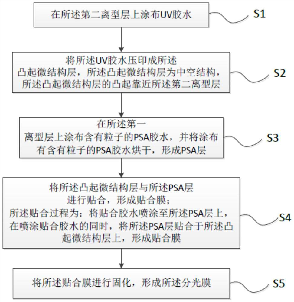
[0071] Such as image 3 As shown, the present invention also provides a method for preparing the above-mentioned spectroscopic film 1, comprising:
[0072] S1, coating UV glue on the second release layer 4;
[0073] S2, embossing the UV glue into a raised microstructure layer 3, the raised microstructure layer 3 is a hollow structure, and the protrusions of the raised microstructure layer 3 are close to the second release layer 4;
[0074] S3. Coating PSA glue containing particles on the first release layer 5, and drying the PSA glue coated with particles to form the PSA layer 2;
[0075] S4, bonding the raised microstructure layer 3 and the PSA layer 2 to form a bonding film;
[0076] The bonding process is as follows: spray the bonding glue onto the PSA layer 2, and bond the PSA layer 2 to the raised microstructure layer 3 while spraying the bonding glue to form a bonding process. membrane;
[0077] S5. Curing the bonding film to form the spectroscopic film.
[0078] Th...
Embodiment 3
[0085] Such as Figure 4 As shown, the present invention also provides a preparation system for the above-mentioned spectroscopic film 1, including:
[0086] Embossing module 11, oven 12, bonding device 13;
[0087] The embossing module 11 is used for embossing the raised microstructure layer 3;
[0088] The imprinting module may include: a working table (not shown in the figure), and an embossing mold 111 for protruding microstructures.
[0089] The workbench is used to place the second release layer 4 coated with UV glue to be embossed;
[0090] The embossed microstructure imprinting mold 111 is as Figure 5 As shown (the raised microstructure only shows the Microlens structure in the figure, it can be understood that the raised microstructure is not limited thereto), the raised microstructure imprint mold 111 is placed above the workbench , for embossing the UV glue to form the raised microstructure layer 3 .
[0091] The oven 12 is used to dry the PSA glue containing ...
PUM
| Property | Measurement | Unit |
|---|---|---|
| Particle size | aaaaa | aaaaa |
| Thickness | aaaaa | aaaaa |
| Thickness | aaaaa | aaaaa |
Abstract
Description
Claims
Application Information


