Double-sided flexible circuit board and manufacturing method thereof

A technology of a flexible circuit board and a manufacturing method, which is applied in the field of flexible circuit boards, can solve the problems of increased cost, insufficient circuit space, large aperture ring, etc., and achieves the effect of reducing the design size

Pending Publication Date: 2022-04-12
SUIWA HIGH TECH ELECTRONICS INDS XIAMEN
View PDF0 Cites 0 Cited by
  • Summary
  • Abstract
  • Description
  • Claims
  • Application Information

AI Technical Summary

Problems solved by technology

When the designed annular ring is insufficient, the etching potion etches the annular ring of the line metal layer from the side and then etches the metal layer in the hole, resulting in the phenomenon of no copper in the hole or holes in the hole in the finished product, resulting in non-conduction defects of the lines on both sides
In order to ensure the reliability of the through-hole connection, a certain amount of the hole ring needs to be reserved in the design of the hole ring to ensure that there will be no broken disk when the circuit layer is etched, resulting in no copper in the hole, which results in a large hole ring and insufficient line space. For some double-sided flexible circuit boards with high-density circuits, it is necessary to increase the product size, resulting in an increase in cost

Method used


Image

  • Double-sided flexible circuit board and manufacturing method thereof
  • Double-sided flexible circuit board and manufacturing method thereof
  • Double-sided flexible circuit board and manufacturing method thereof

Examples


Embodiment Construction

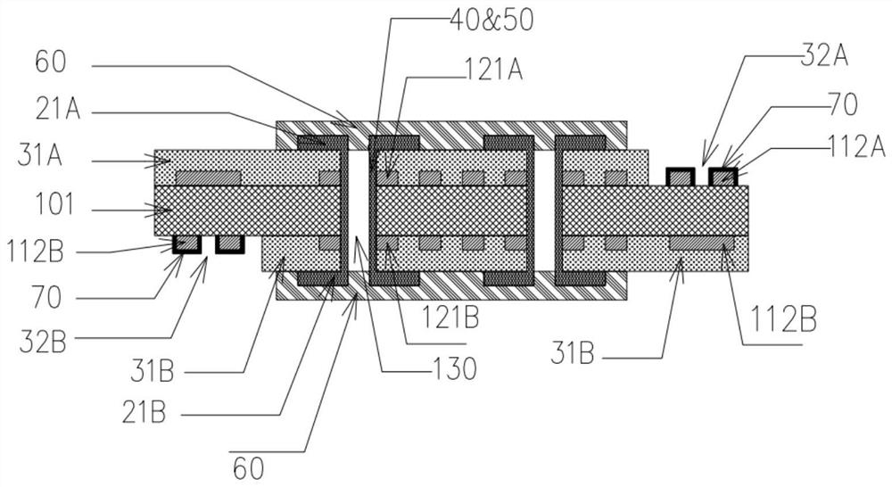
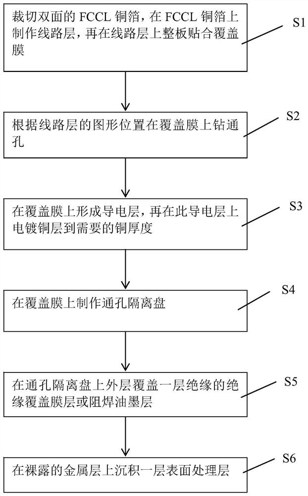
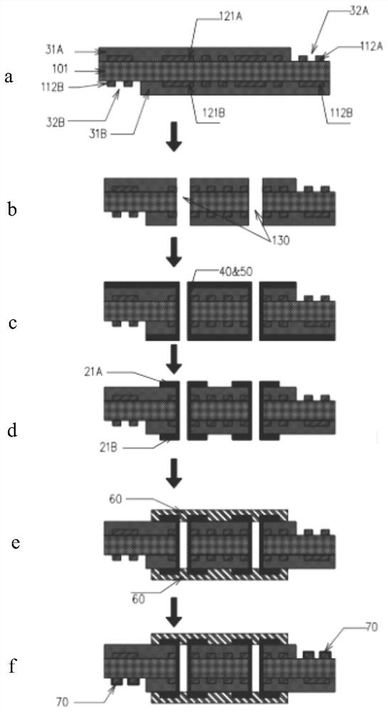
[0020] It should be noted that the experimental methods described in the following embodiments, unless otherwise specified, are conventional methods, and the reagents and materials, unless otherwise specified, can be obtained from commercial sources; in the description of the present application, The terms "landscape", "portrait", "top", "bottom", "front", "rear", "left", "right", "vertical", "horizontal", "top", "bottom", The orientation or positional relationship indicated by "inner", "outer", etc. is based on the orientation or positional relationship shown in the drawings, which is only for the convenience of describing the present invention and simplifying the description, and does not indicate or imply that the referred device or element must have Certain orientations, constructed and operative in certain orientations, therefore are not to be construed as limitations on the invention.

[0021] In addition, the terms "horizontal", "vertical", "overhanging" and the like do...


PUM


Abstract

The invention relates to a double-sided flexible circuit board and a manufacturing method thereof, and the method comprises the following steps: S1, cutting a double-sided FCCL copper foil, manufacturing a circuit layer on the double-sided FCCL copper foil, and attaching a cover film to the whole circuit layer; s2, drilling a through hole in the covering film according to the pattern position of the circuit layer; s3, forming a conductive layer on the covering film, and electroplating a copper layer on the conductive layer to a required copper thickness; s4, manufacturing a through hole isolation disc on the covering film, and manufacturing a required pattern on the product by using an anti-etching dry film according to the position of the circuit pattern layer; s5, covering an insulating cover film layer or a solder resist ink layer on the outer layer of the through hole isolation disc; and S6, depositing a surface treatment layer on the exposed circuit layer. According to the manufacturing method, the circuit is manufactured firstly, then the through hole is manufactured, etching liquid medicine cannot be etched to the metal layer in the hole from the side face, the design size of the hole ring of the circuit layer is reduced in the state that the hole diameter of the through hole cannot be reduced, and the defect that the hole ring is large in a conventional manufacturing mode can be overcome.

Description

technical field [0001] The invention relates to the field of flexible circuit boards, in particular to a double-sided flexible circuit board and a manufacturing method thereof. Background technique [0002] The conventional production process of double-sided flexible circuit board is to make through holes first, then make the circuit layer, and then make the surface structure layer (cover film, solder resist ink, surface treatment, etc.). Because the through hole is made first and then the circuit layer is made, when the subtractive method is used, the etching solution will also etch the side when it is etched downward. When the designed annular ring is insufficient, the etching potion etches the annular ring of the line metal layer from the side and then etches the metal layer in the hole, resulting in the phenomenon of no copper in the hole or holes in the hole in the finished product, resulting in non-conduction defects of the lines on both sides. In order to ensure the ...

Claims


Application Information

Patent Timeline
Patent Type & Authority Applications(China)
IPC IPC(8): H05K3/00
Inventor 石丽丽曹先贵王小娟
Owner SUIWA HIGH TECH ELECTRONICS INDS XIAMEN
Why Eureka
Try Eureka