Conductive device with superconductive narrow frame and directional ultrasonic transparent screen
A technology of conductive device and narrow frame, applied in conductive layer on insulating carrier, electrical digital data processing, input/output process of data processing, etc., to increase conductivity, reduce total light transmittance, and improve sound pressure performance Effect
- Summary
- Abstract
- Description
- Claims
- Application Information
AI Technical Summary
Problems solved by technology
Method used
Image


Examples
Embodiment 1
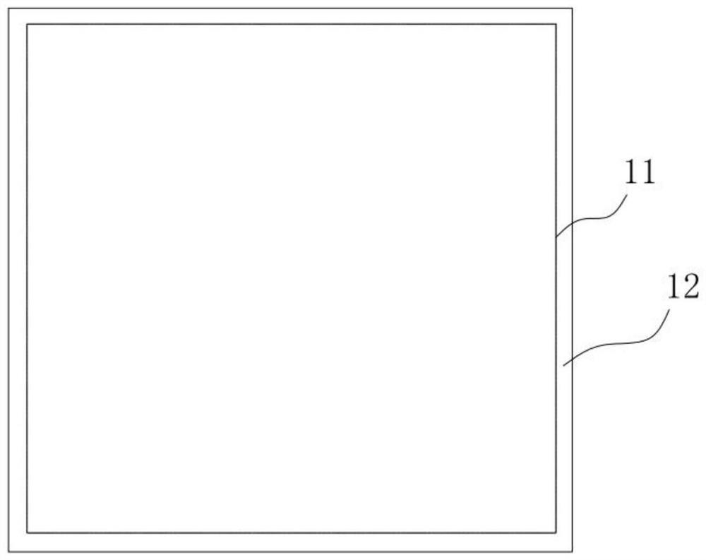
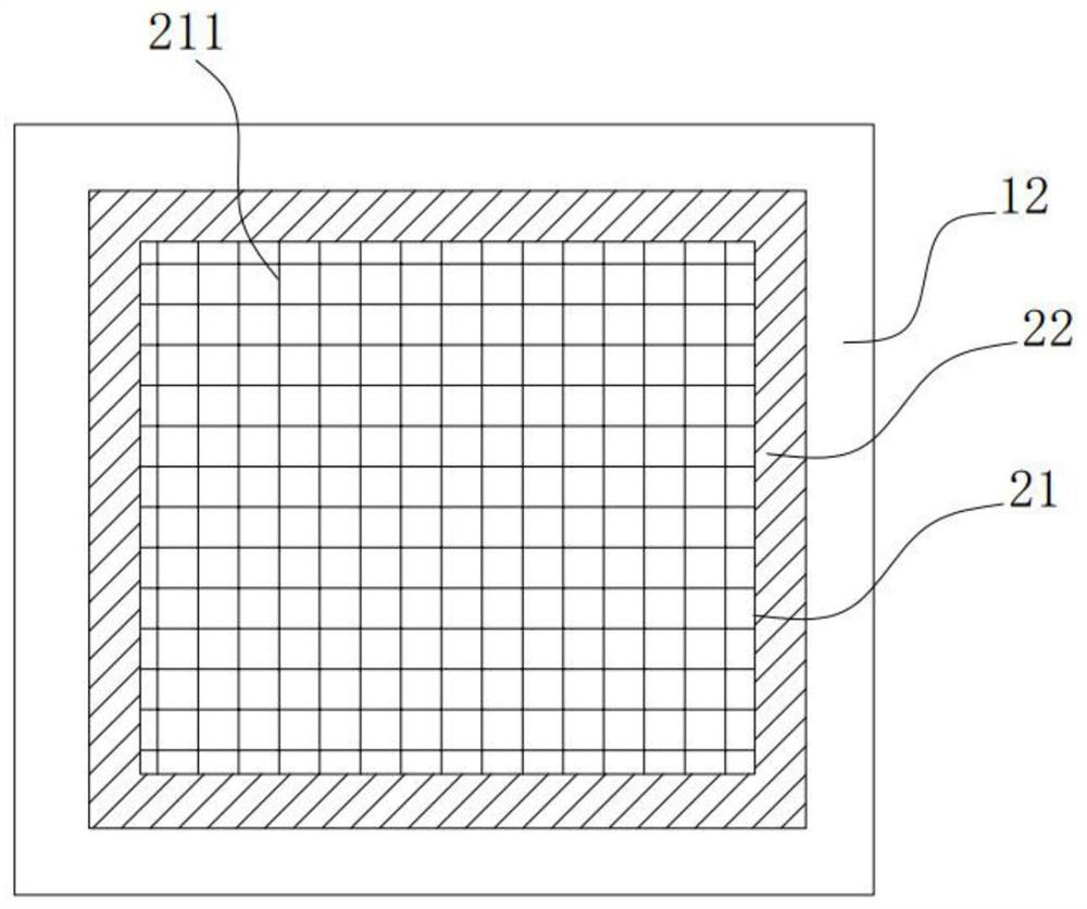
[0041] like Figure 5 As shown, a conductive device with a superconducting narrow frame disclosed in Embodiment 1 of the present invention includes a conductive base 1, a first conductive layer and a second conductive layer, wherein the first conductive layer is disposed on the conductive base 1, and the second The two conductive layers are disposed on the first conductive layer. Wherein, the first conductive layer is copper wiring, combined with image 3 As shown, it includes an in-plane conductive layer 21 and a frame conductive layer 22, and the in-plane conductive layer 21 and the frame conductive layer 22 are preferably realized in one operation. Specifically, the entire surface of the conductive substrate 1 is sputtered to form a layer of copper, and then the in-plane conductive layer 21 and the frame conductive layer 22 are formed by exposure and development. In this way, the in-plane conductive layer The thickness of 21 is the same as that of the frame conductive lay...
Embodiment 2
[0046] like Figure 6 As shown, a conductive device with a superconducting narrow frame disclosed in Embodiment 2 of the present invention includes a conductive base 1, a first conductive layer and a second conductive layer, wherein the first conductive layer is disposed on the conductive base, and the second The conductive layer is disposed on the first conductive layer. Wherein, when the first conductive layer is implemented, indium tin oxide or nano-silver wire can be used, and specifically, it can be formed on the conductive substrate 1 by spraying or sputtering. The second conductive layer is a copper wire, which includes an in-plane conductive layer 21 and a frame conductive layer 22 , and the in-plane conductive layer 21 and the frame conductive layer 22 are preferably implemented in one operation. Specifically, the entire surface of the first conductive layer is sputtered to form a layer of copper first, and then the in-plane conductive layer 21 and frame conductive l...
Embodiment 3
[0050] like Figure 7 As shown, a conductive device with a superconducting narrow frame disclosed in Embodiment 3 of the present invention includes a conductive substrate 1, a first conductive layer and a second conductive layer, wherein the first conductive layer is disposed on the conductive substrate 1, and the second conductive layer The two conductive layers are disposed on the first conductive layer. Wherein, the first conductive layer is a metal grid, which includes an in-plane conductive layer 21 and a border conductive layer 22 . Specifically, in order to ensure the visual effect, the metal line width of the metal mesh of the in-plane conductive layer 21 should be more than 20 μm, the distance between two adjacent metal traces is greater than 200 μm, and the thickness of the in-plane conductive layer 21 can be Reaching the nanometer level, the thickness and the width of the metal trace can be calculated according to the value of the loaded current. In order to ensur...
PUM
| Property | Measurement | Unit |
|---|---|---|
| Width | aaaaa | aaaaa |
| Thickness | aaaaa | aaaaa |
| Width | aaaaa | aaaaa |
Abstract
Description
Claims
Application Information
 - R&D
- Intellectual Property
- Life Sciences
- Materials
- Tech Scout
- Unparalleled Data Quality
- Higher Quality Content
- 60% Fewer Hallucinations
Browse by: Latest US Patents, China's latest patents, Technical Efficacy Thesaurus, Application Domain, Technology Topic, Popular Technical Reports.
© 2025 PatSnap. All rights reserved.Legal|Privacy policy|Modern Slavery Act Transparency Statement|Sitemap|About US| Contact US: help@patsnap.com