


Quick Research
Generate reliable direction feasibility study reports for your R&D in just a few steps.

Technical Q&A
Discover and master advanced knowledge NOW. Basics, ideas, possibilities, all at once.

Find Solutions
As an expert in R&D theories, this can generate solutions to your technical problems instantly.

Evaluate Feasibility
Analyze your overall solution with one click, know your potential R&D risks in advance.

Monitor Landscape
Get weekly tech updates, stay abreast of the latest tech innovations and key insights.
Surface conformal array design method based on transformation optics and neural network algorithm
A neural network algorithm and conformal array technology, applied in the field of artificial electromagnetic devices, can solve problems such as difficult array element positions and inaccurate results
- Summary
- Abstract
- Description
- Claims
- Application Information
AI Technical Summary
Problems solved by technology
Method used
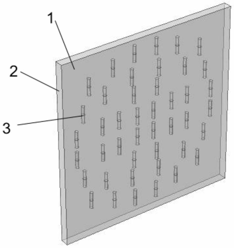
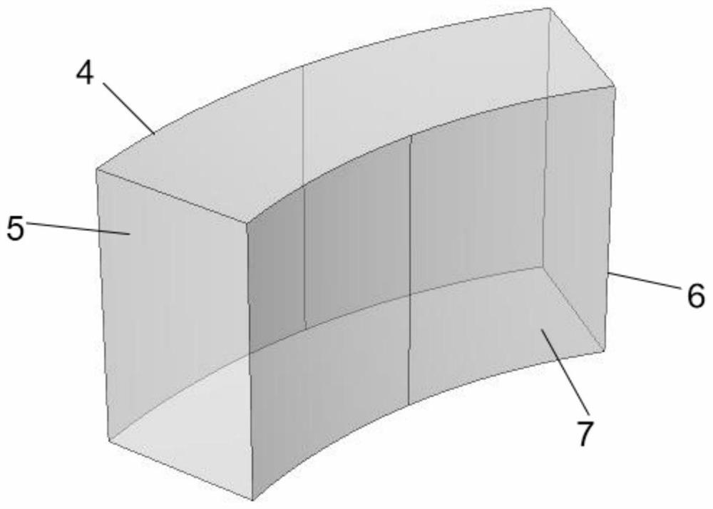
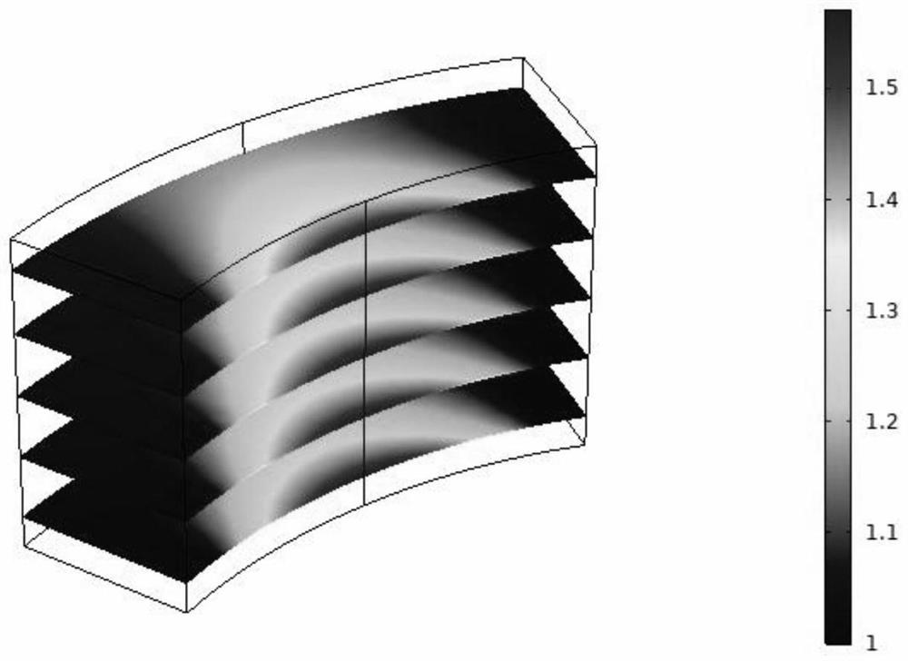
Image

Examples
Embodiment Construction
[0066] In order to make the problems to be solved by the present invention and the effects clearer and clearer, the present invention will be further described below in conjunction with the accompanying drawings and embodiments. It should be understood that the specific embodiments described here are only used to explain the present invention, but not to limit the present invention.
[0067] The specific steps and implementation details of the embodiment of the present invention are as follows:
[0068] Step 1: Apply the 2D-UMP planar array optimization algorithm to the planar array, so as to obtain the array element position and array element excitation size of the optimized planar array in the virtual space. Embodiments First, the 2D-UMP planar array optimization algorithm is used to sparsely optimize the Chebyshev array to obtain the sparse planar array position and excitation. Assume that the planar array factors are:
[0069]
[0070] Among them, p represents a certa...
PUM
 Abstract
Description
Claims
Application Information
 - R&D Engineer
- R&D Manager
- IP Professional
- Industry Leading Data Capabilities
- Powerful AI technology
- Patent DNA Extraction
Browse by: Latest US Patents, China's latest patents, Technical Efficacy Thesaurus, Application Domain, Technology Topic, Popular Technical Reports.
© 2024 PatSnap. All rights reserved.Legal|Privacy policy|Modern Slavery Act Transparency Statement|Sitemap|About US| Contact US: help@patsnap.com