Supercharge Your Innovation With Domain-Expert AI Agents!

5G optical module PCB punching device capable of adjusting drilling size

A drilling device and optical module technology, applied in metal processing, etc., can solve the problems affecting production efficiency, unable to change the drilling aperture independently, etc.

Inactive Publication Date: 2022-04-29
益阳市明正宏电子有限公司
View PDF4 Cites 0 Cited by
  • Summary
  • Abstract
  • Description
  • Claims
  • Application Information

AI Technical Summary

Problems solved by technology

[0004] In the current existing technology, the drilling equipment for PCB cannot change the drilling aperture independently during the production process. When the drilling aperture needs to be changed, the drill bit needs to be replaced manually, which affects the production efficiency; for this reason, the present invention provides a 5G optical module PCB drilling device for adjusting the drilling size

Method used


Image

  • 5G optical module PCB punching device capable of adjusting drilling size
  • 5G optical module PCB punching device capable of adjusting drilling size
  • 5G optical module PCB punching device capable of adjusting drilling size

Examples


Embodiment 1

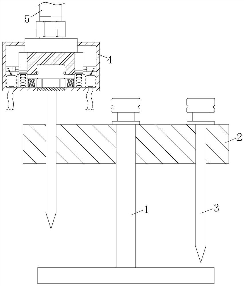
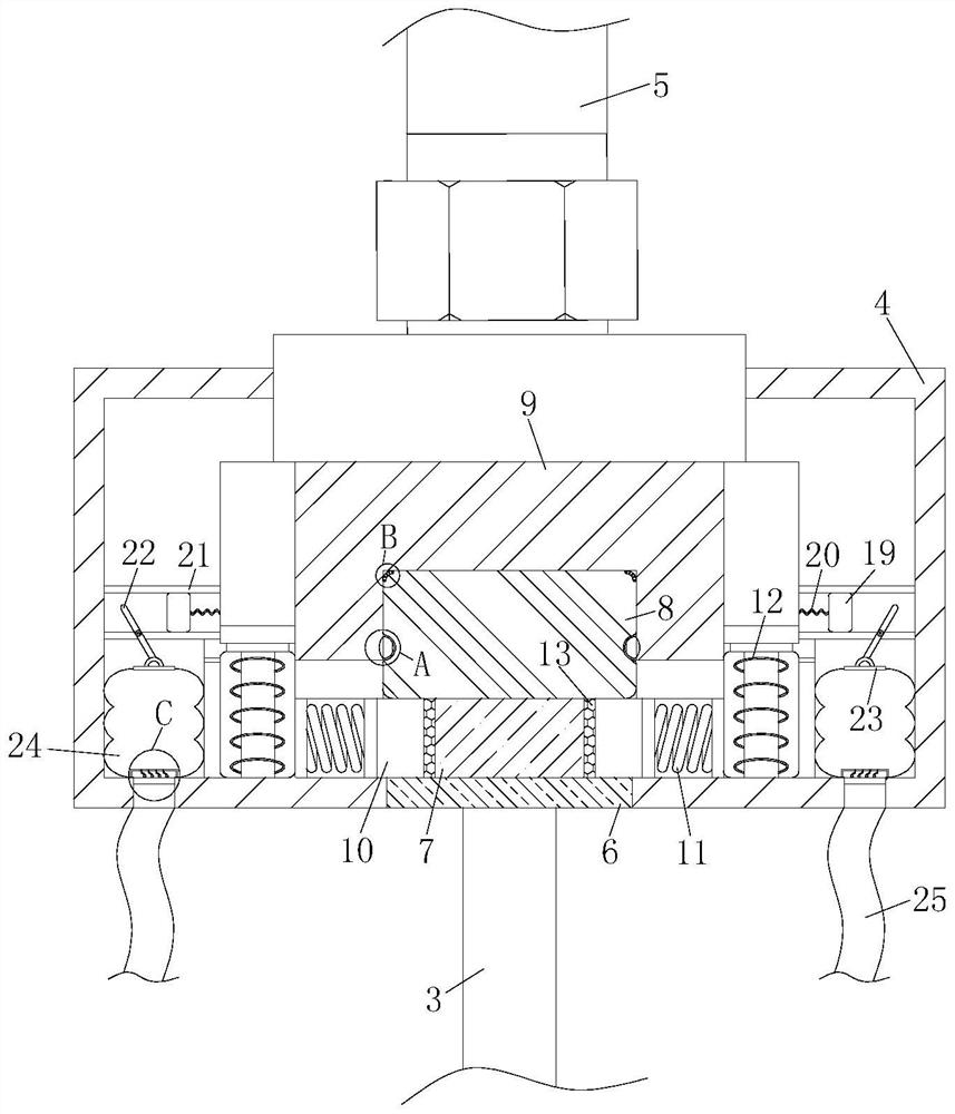
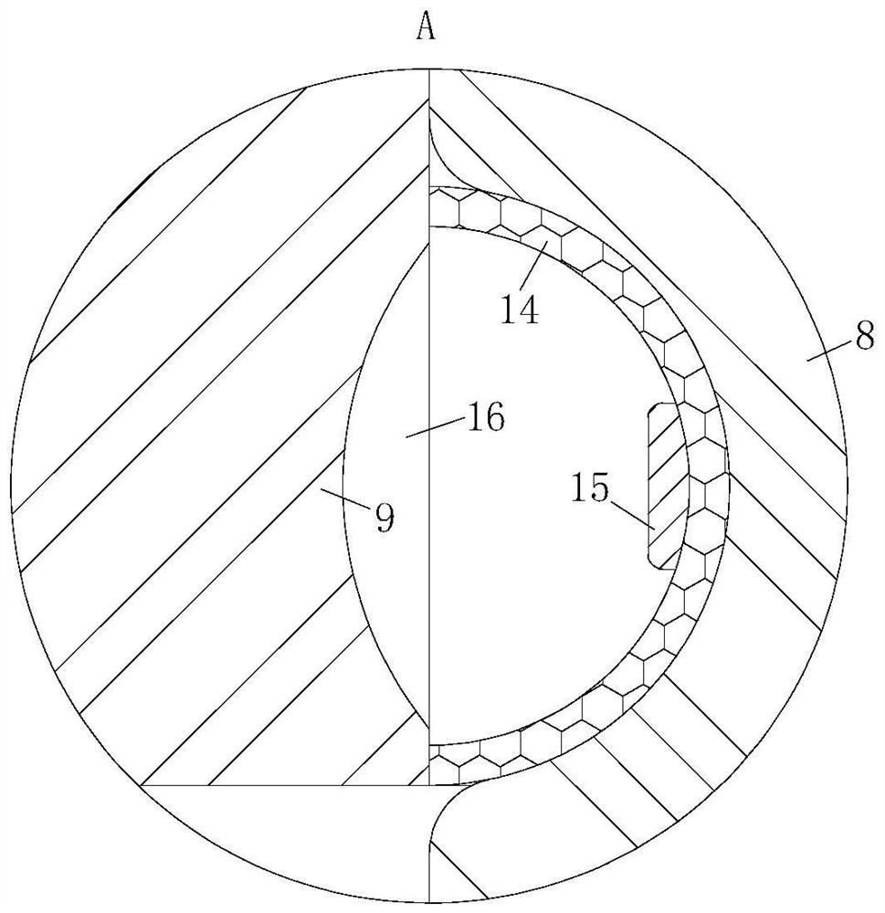
[0030] Such as Figure 1 to Figure 2 As shown, a 5G optical module PCB drilling device for adjusting the drilling size described in the embodiment of the present invention includes a rotating shaft 1, and a mounting plate 2 is fixed on the upper end of the rotating shaft 1, and the mounting plate 2 is connected internally. There are multiple groups of drill bits 3, and the diameters of the multiple groups of drill bits 3 are not equal. A fastening housing 4 is arranged above the drill bits 3, and a transmission rod 5 is fixed on the upper end of the fastening housing 4; during work, the servo The drive module will drive the transmission rod 5 to rotate, and the rotating shaft 1 rotates to drive the fastening housing 4 to rotate, and the fastening housing 4 rotates to drive the drill bit 3 to rotate to drill the PCB. When the drilling size needs to be adjusted, this In this case, data equipment is required to drive the transmission rod 5 to the top of the rotating shaft 1, then...

Embodiment 2

[0040] Such as Figure 6 to Figure 7 As shown in Comparative Example 1, another embodiment of the present invention is: a detection contact 29 is slidably connected to the top of the clamping block 8, and a detection contact 29 is fixed between the detection contact 29 and the clamping block 8. A spring 31, a circuit contact 30 is arranged above the detection contact 29, and the circuit contact 30 is fixedly connected to the connecting block 9; during operation, during the installation of the clamping block 8, it will simultaneously drive its internal The detection contact 29 is in contact with the circuit contact 30, and the setting of the detection spring 31 can make buffering during the contact process, and also makes the detection contact 29 contact with the circuit contact 30 more closely after the installation is completed, and different The detection contact 29 on the drill bit 3 is different to the signals transmitted by the system, thereby facilitating the system to j...


PUM


Abstract

The invention belongs to the technical field of printed circuit board (PCB) manufacturing, and particularly relates to a 5G optical module PCB punching device capable of adjusting the drilling size. The 5G optical module PCB punching device comprises a rotating shaft, a mounting disc is fixed to the upper end of the rotating shaft, multiple sets of drill bits are connected to the interior of the mounting disc in a penetrating mode, the diameters of the multiple sets of drill bits are different, a fastening shell is arranged above the drill bits, and the fastening shell is connected with the rotating shaft. A transmission rod is fixed to the upper end of the fastening shell, a fastening block is fixed to the upper end of the drill bit, a clamping block is fixed to the upper end of the fastening block, a connecting block is slidably connected to the outer portion of the clamping block, the connecting block is fixedly connected with the fastening shell, and an elastic ring piece is fixed to the inner wall of the connecting block. A groove matched with the elastic ring piece is formed in the outer portion of the clamping block. The fastening shell is controlled to move through the numerical control drilling equipment, and the mounting disc is driven to rotate through the rotating shaft, so that a drill bit is replaced, the drilling size can be effectively changed, and the effect of adjusting the drilling size is achieved.

Description

technical field [0001] The invention belongs to the technical field of printed circuit board (PCB) manufacturing, and specifically relates to a 5G optical module PCB drilling device for adjusting the drilling size. Background technique [0002] PCB is a printed circuit board that people often say, and it plays an extremely important role in electronic components. Nowadays, with the rapid development of 5G signals, in order to meet people's needs for 5G signals, it is often necessary to install 5G optical components on PCBs. Modules, which require holes to be reserved in advance during the PCB manufacturing process. [0003] A Chinese patent with the publication number CN104582238A discloses a PCB board and its manufacturing method. The PCB board includes: an outer layer with at least two detection holes; at least one inner layer arranged between the outer layers, including a test A strip and a back-drilling hole formed by a back-drilling process, the test strip includes a t...

Claims


Application Information

Patent Timeline
IPC IPC(8): B26F1/16B26D7/26B26D7/02
CPCB26F1/16B26D7/2628B26D7/02
Inventor 邬家康祝文华郭胜涛李显刚陈泽和胡珊珊
Owner 益阳市明正宏电子有限公司
Features
  • R&D
  • Intellectual Property
  • Life Sciences
  • Materials
  • Tech Scout
  • Unparalleled Data Quality
  • Higher Quality Content
  • 60% Fewer Hallucinations
Learn More