Method for forming IGBT electric field stop layer

A technology of electric field termination layer and substrate, which is applied in circuits, electrical components, semiconductor devices, etc., and can solve problems affecting IGBT reliability, IGBT turn-off oscillation, etc.

Pending Publication Date: 2022-05-03
权芯微电子科技无锡有限公司
View PDF0 Cites 1 Cited by
  • Summary
  • Abstract
  • Description
  • Claims
  • Application Information

AI Technical Summary

Problems solved by technology

[0003] To form the electric field termination layer of the IGBT, the current method is to thin the substrate to the required thickness after the front side of the IGBT is processed, then inject P on the back side, and then activate it by laser annealing, at a depth of 1-2um on the back side of the substrate Within the range, the N-type impurity distribution with increased concentration, that is, the electric field termination layer, is formed, so as to improve the IGBT withstand voltage. Although the electric field termination layer formed by this method can play the role of withstand voltage, but due to the depth of the electric field termination layer Only 1-2um, the current drops rapidly when the IGBT is turned off, causing oscillation when the IGBT is turned off, thus affecting the reliability of the IGBT

Method used


Image

  • Method for forming IGBT electric field stop layer
  • Method for forming IGBT electric field stop layer
  • Method for forming IGBT electric field stop layer

Examples


Embodiment

[0041] like Figure 1-13 As shown, an embodiment of the present invention provides a method for forming an electric field stop layer of an IGBT, and the method includes the following steps:

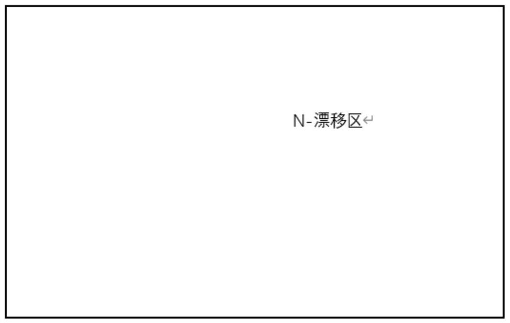
[0042] S1. Substrate preparation, the substrate is a uniformly doped N-type silicon-based substrate (see figure 1 );

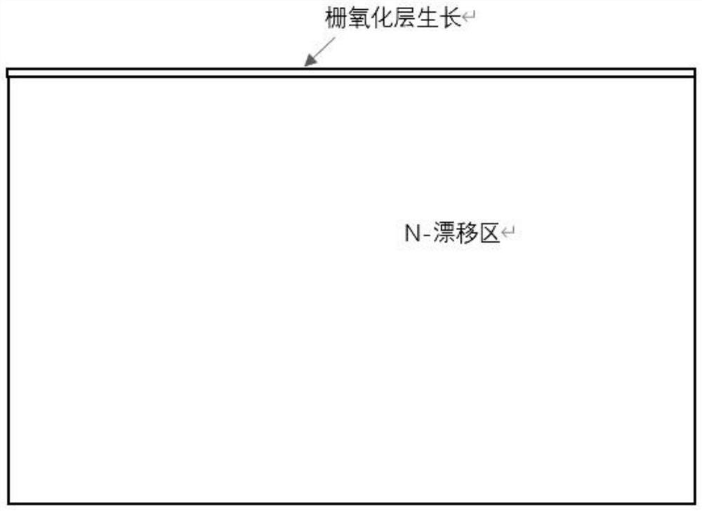
[0043] S2, the growth of gate oxide layer, the condition is 1100-1150 ℃ dry oxygen growth method (see figure 2 );

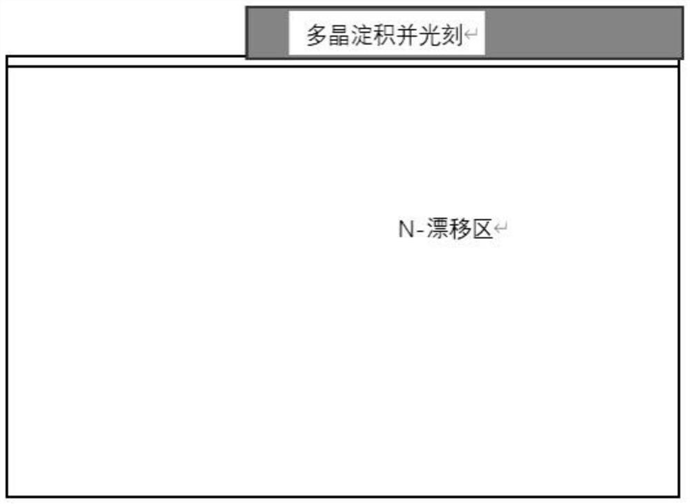
[0044] S3, polycrystalline deposition and photolithography, the thickness of the deposited polycrystalline is about 1um, and the sheet resistance after doping is 4-16ohm / sq (see image 3 );

[0045] S4, P-type body region implantation, for B impurity implantation, the implantation dose is 2-10e13 / cm 2 , the injection energy is 60-100Kev (see Figure 4 );

[0046] S5, P-type body area push, push temperature is 1150 ℃, time is 90-120min (see Figure 5 );

[0047] S6, N+ is injected and pushed, and As is injected, the dose is 5e15 / cm 2 -10e15 / cm 2 ,...


PUM


Abstract

The invention provides a method for forming an IGBT electric field stop layer, and relates to the technical field of IGBT processes. The method for forming the IGBT electric field stop layer comprises the following steps: S1, preparing a substrate; s2, growing a gate oxide layer; s3, polycrystal deposition and photoetching are carried out; s4, injecting a P-type body region; s5, propelling a P-type body region; s6, performing N + injection and propulsion; s7, depositing a dielectric layer; s8, performing contact hole photoetching and metal sputtering; s9, injecting a P-type collector region on the back surface; s10, annealing a collector region on the back surface; s11, high-energy protons are injected into the back surface for many times; s12, performing high-energy proton injection annealing; and S13, back collector electrode metal sputtering is carried out. According to the method, high-energy proton injection is carried out for many times, then annealing is carried out at the temperature of 350-450 DEG C and under the N2 condition, N-type impurity distribution with the thickness of 20-50 microns is formed on the back face of the IGBT, and therefore the function of an electric field stop layer is achieved, due to the fact that the number of electrons in the thick electric field stop layer is large, the current cannot suddenly drop to zero when the IGBT is turned off, and oscillation of the IGBT cannot be caused.

Description

technical field [0001] The invention relates to the technical field of IGBT technology, in particular to a method for forming an electric field termination layer of an IGBT. Background technique [0002] The static and dynamic power consumption requirements of IGBTs are getting lower and lower, and reducing the thickness of IGBTs is an effective method to achieve this purpose. In order to maintain the withstand voltage capability of IGBTs, forming an electric field termination layer on the back of IGBTs is an effective method to maintain withstand voltages of IGBTs. [0003] To form the electric field termination layer of the IGBT, the current method is to thin the substrate to the required thickness after the front side of the IGBT is processed, then inject P on the back side, and then activate it by laser annealing to a depth of 1-2um on the back side of the substrate Within the range, an N-type impurity distribution with an increased concentration is formed, that is, an e...

Claims


Application Information

Patent Timeline
Patent Type & Authority Applications(China)
IPC IPC(8): H01L21/331H01L21/324H01L29/739
CPCH01L29/66333H01L29/7395H01L21/324
Inventor 李云燕
Owner 权芯微电子科技无锡有限公司
Why Eureka
Try Eureka