Unlock instant, AI-driven research and patent intelligence for your innovation.

PCB defect detection method, apparatus and device, and storage medium

A defect detection and defect technology, applied in the field of defect detection, can solve problems such as inability to accurately classify PCBs, and achieve the effect of improving accuracy and universality

Pending Publication Date: 2022-05-10
阿丘机器人科技(苏州)有限公司
View PDF0 Cites 1 Cited by
  • Summary
  • Abstract
  • Description
  • Claims
  • Application Information

AI Technical Summary

Problems solved by technology

[0004] The main purpose of the present invention is to provide a PCB defect detection method, device, equipment and storage medium, aiming to solve the technical problem that the prior art cannot accurately classify PCB defects

Method used


Image

  • PCB defect detection method, apparatus and device, and storage medium
  • PCB defect detection method, apparatus and device, and storage medium
  • PCB defect detection method, apparatus and device, and storage medium

Examples


Embodiment Construction

[0049] It should be understood that the specific embodiments described here are only used to explain the present invention, not to limit the present invention.

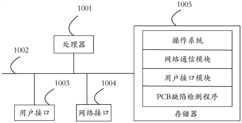
[0050] refer to figure 1 , figure 1 It is a schematic structural diagram of a PCB defect detection device in the hardware operating environment involved in the solution of the embodiment of the present invention.

[0051] like figure 1 As shown, the PCB defect detection device may include: a processor 1001 , such as a central processing unit (Central Processing Unit, CPU), a communication bus 1002 , a user interface 1003 , a network interface 1004 , and a memory 1005 . Wherein, the communication bus 1002 is used to realize connection and communication between these components. The user interface 1003 may include a display screen (Display), an input unit such as a keyboard (Keyboard), and the optional user interface 1003 may also include a standard wired interface and a wireless interface. The network interface 100...


PUM


Abstract

The invention discloses a PCB defect detection method, device and equipment and a storage medium, and the method comprises the steps: inputting a product picture of a to-be-detected PCB product into a preset neural network model, and obtaining the defect information of the to-be-detected PCB product; obtaining a preset defect release standard, and comparing the defect information with the preset defect release standard to obtain a defect comparison result; and according to a defect comparison result, judging whether the to-be-detected PCB product has a releasable defect or not. According to the method, the product picture of the to-be-detected PCB product is input into the preset neural network model to obtain the defect information of the to-be-detected PCB product, the defect information is compared with the preset direction defect standard to obtain the defect comparison result, and whether the to-be-detected PCB product has the releasable defect or not is judged according to the comparison result. The defects of the PCB product can be accurately classified, the requirements of different customers for the product quality can be met, and the accuracy and universality of PCB defect detection are improved.

Description

technical field [0001] The present invention relates to the technical field of defect detection, in particular to a PCB defect detection method, device, equipment and storage medium. Background technique [0002] In terms of existing PCB appearance defect detection, it is difficult to detect the existence of different defects caused by various production processes. As designers and manufacturers put forward higher and higher requirements for product quality, users' demand and requirements for appearance inspection equipment are getting higher and higher. In recent years, with the development of machine vision technology, more and more equipment manufacturers have launched PCB appearance inspection equipment with different precision. The detection algorithm based on traditional machine vision cannot accurately classify PCB defects and cannot flexibly respond to different quality requirements of different customers. Therefore, how to accurately classify PCB defects has become...

Claims


Application Information

Patent Timeline
IPC IPC(8): G06T7/00G06V10/764G06V10/82G06K9/62G06N3/04G06N3/08
CPCG06T7/0004G06N3/04G06N3/08G06T2207/20081G06T2207/20084G06T2207/30141G06F18/241
Inventor 黄耀张峰
Owner 阿丘机器人科技(苏州)有限公司