

Parameter optimization method and system of analog integrated circuit
A technology of integrated circuits and optimization methods, applied in the fields of electrical digital data processing, computational models, character and pattern recognition, etc., can solve the loss of use value, increase the difficulty of Bayesian optimization algorithm high-dimensional problems, and Bayesian optimization algorithm iteration The number of times is limited to avoid excessive computing resource overhead, improve optimization efficiency, and increase the number of iterations.
- Summary
- Abstract
- Description
- Claims
- Application Information
AI Technical Summary
Problems solved by technology
Method used
Image

Examples
Embodiment Construction
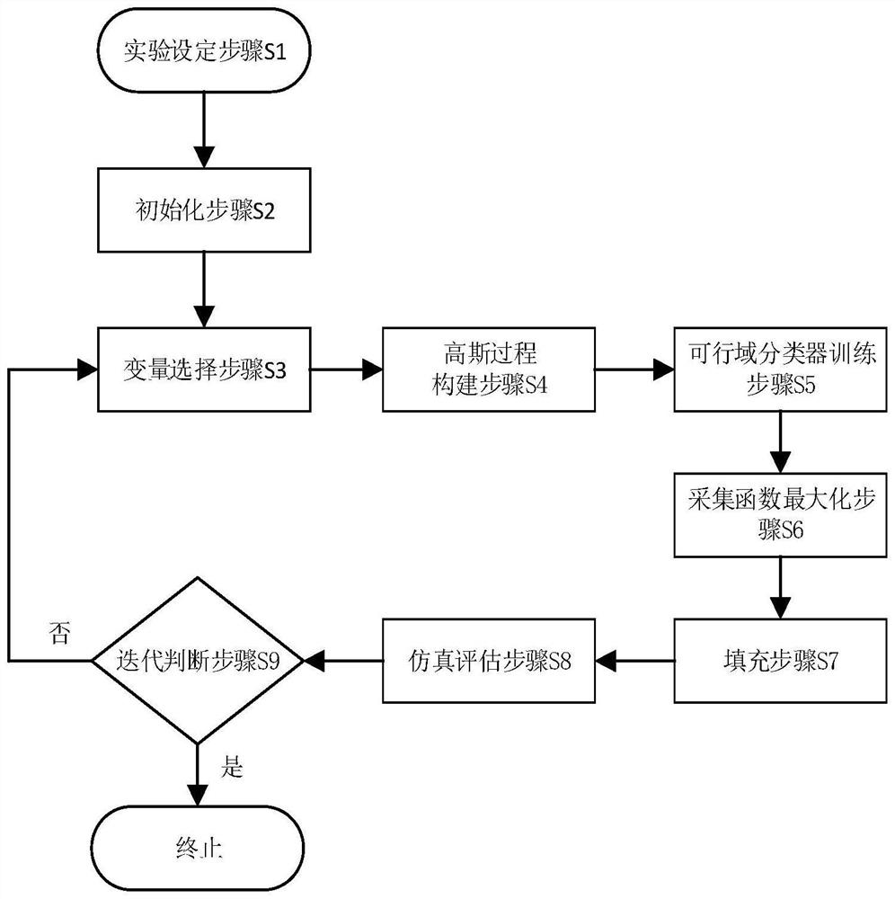
[0047] In order to enable those skilled in the art to better understand the solutions of the present invention, the following will clearly and completely describe the technical solutions in the embodiments of the present invention in conjunction with the drawings in the embodiments of the present invention. Obviously, the described embodiments are only It is an embodiment of a part of the present invention, but not all embodiments. Based on the embodiments of the present invention, all other embodiments obtained by persons of ordinary skill in the art without making creative efforts shall fall within the protection scope of the present invention.
[0048] It should be noted that the terms "first" and "second" in the description and claims of the present invention and the above drawings are used to distinguish similar objects, but not necessarily used to describe a specific sequence or sequence. It is to be understood that the data so used are interchangeable under appropriate ...
PUM
 Abstract
Description
Claims
Application Information