An intelligent test system, method and medium for a light-emitting diode

A technology of light emitting diodes and testing methods, which is applied in testing optical performance, single semiconductor device testing, and electrical measurement, etc., can solve the problems of chip damage, high defective rate, damage, etc., so as to reduce the defective rate and improve the detection efficiency. Efficiency and the effect of improving the genuine rate

Active Publication Date: 2022-06-24
深圳市粉紫实业有限公司
View PDF8 Cites 0 Cited by
  • Summary
  • Abstract
  • Description
  • Claims
  • Application Information

AI Technical Summary

Problems solved by technology

[0003] Nowadays, the detection efficiency of light-emitting diodes is still low, and in actual application scenarios, the detection standard is too simple, so there are still many problems in the light-emitting diodes after detection. For example, the chips inside the light-emitting diodes are mainly made of solder. The way of bonding, but a lot of heat will be generated in the process of solder bonding, which will cause damage to the chip and affect the overall performance of the light-emitting diode. There is no such damage detection in the prior art.
Moreover, in the prior art, there is a lack of detection of damage to parts inside the light-emitting diodes. Most of the factory inspections of light-emitting diodes only stop at the detection of light intensity, and the detection of light-emitting diodes is not thorough enough. As a result, the light-emitting diodes after leaving the factory are still There are some defective products, and the defective rate is too high

Method used


Image

  • An intelligent test system, method and medium for a light-emitting diode
  • An intelligent test system, method and medium for a light-emitting diode
  • An intelligent test system, method and medium for a light-emitting diode

Examples


Embodiment Construction

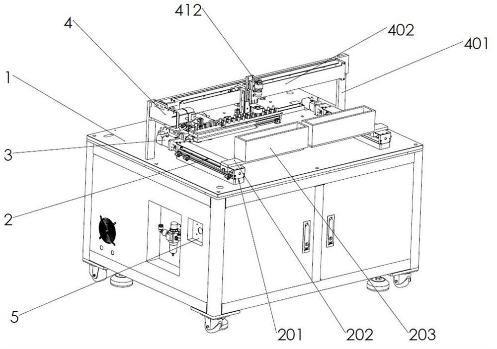
[0055] In order to be able to more clearly understand the above objects, features and advantages of the present invention, the present invention will be further described in detail below with reference to the accompanying drawings and specific embodiments. Therefore, it only shows the structure related to the present invention, and it should be noted that the embodiments of the present application and the features of the embodiments can be combined with each other without conflict.

[0056] In the description of this application, it should be understood that the terms "center", "portrait", "horizontal", "top", "bottom", "front", "rear", "left", "right", " The orientations or positional relationships indicated by vertical, horizontal, top, bottom, inner, and outer are based on the orientations or positional relationships shown in the accompanying drawings, and are only for the convenience of describing the present application and The description is simplified rather than indica...


PUM


Abstract

The present invention relates to an intelligent testing system, method and medium of light-emitting diodes, belonging to a testing device for light-emitting diodes, including a frame, at least two sets of storage modules arranged in parallel on the frame, a testing module, a feeding module and The control terminal, the test module includes a third linear movement module arranged on the frame, a fourth linear movement module is arranged on the third linear movement module, and a fourth linear movement module is arranged on the fourth linear movement module. The third moving block, the two sides of the third moving block are provided with a second moving cylinder, the output end of the second moving cylinder is provided with a test platform, and a plurality of probes are arranged on the test platform, and the probes Used to contact the positive and negative terminals of the LED so that the probe can communicate with the internal components of the LED. The faults of the internal parts of the light emitting diode can be quickly detected through the probe, thereby screening out unqualified products and improving the authenticity rate of the miniature light emitting diodes when they leave the factory.

Description

technical field [0001] The invention relates to the field of light-emitting diode testing, in particular to an intelligent testing system, method and medium for light-emitting diodes. Background technique [0002] With the country's policy and financial support for the semiconductor industry, as well as the continuous increase in technological investment and development of domestic semiconductor industry manufacturers, the proportion of my country's semiconductor market in the world's semiconductor market has continued to expand, and the process of domestic substitution of semiconductor products has gradually accelerated. Light-emitting diodes, referred to as LEDs, as one of the most basic light-emitting devices, play an indispensable role in the field of display lighting in today's society. With the development of society, in the field of display and lighting, people have put forward higher requirements for LED devices. The ideal LED device should be the unity of external ...

Claims


Application Information

Patent Timeline
Patent Type & Authority Patents(China)
IPC IPC(8): G01R31/26G01R1/04G01M11/02G06V20/00G06V10/82G06N3/04
CPCG01R31/2601G01R1/0408G01M11/02G06N3/045Y02E10/50
Inventor 林灿标
Owner 深圳市粉紫实业有限公司
Why Eureka
Try Eureka