Single-phase inverter and control method and control system thereof

A single-phase inverter, source inverter technology

Pending Publication Date: 2022-05-17
GUANGDONG ZHICHENG CHAMPION GROUP
1 Cites 3 Cited by

AI-Extracted Technical Summary

Problems solved by technology

Although the topology proposed in this patent improves the gain of the original inverter, it introduces too many switching devices, which obviously increases the cost, which is not conducive to low-cost industrial applications.
In addition, its control is relatively complicated, and ...

Abstract

The invention discloses a single-phase inverter and a control method and system thereof, and the single-phase inverter comprises a Semi-Z source inverter. The input source is connected with the input side of the Semi-Z source inverter; the boosting module is connected with the output side of the Semi-Z source inverter; and the filtering module is connected with the boosting module. The invention provides an improved topology and control for a Semi-Z source inverter topology, and a novel double-end common-ground single-phase inverter is combined with the Semi-Z source inverter, so that the limitation that the gain is 1 is broken through, and high gain is realized, that is, the positive gain is infinite, and the negative gain is also infinite.

Application Domain

Efficient power electronics conversionApparatus without intermediate ac conversion +2

Technology Topic

Inverter topologyZ-source inverter +5

Image

  • Single-phase inverter and control method and control system thereof
  • Single-phase inverter and control method and control system thereof
  • Single-phase inverter and control method and control system thereof

Examples

  • Experimental program(1)

Example Embodiment

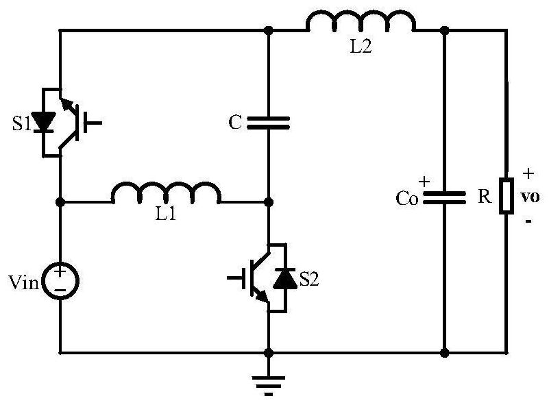
[0041] The topology of the novel high-gain dual-terminal common-ground single-phase inverter based on the Semi-Z source inverter proposed in Embodiment 1 of the present invention is as follows: Figure 4 shown. by the input source V in , inductance L 1 , inductance L 2 , inductance L 3 , inductance L 4 , capacitance C 1 , capacitance C 2 , capacitance C o , switch tube S 1 , switch tube S 2 and switch tube S 3 and so on. where the capacitor C 1 , capacitance C 2 , inductance L 1 , inductance L 2 , switch tube S 2 and switch tube S 3 Constitutes a Semi-Z source inverter. In the inverter part, it can be seen from the Semi-Z source inverter that the switch tube S 2 and switch tube S 3 cannot be turned on at the same time. Similarly, for the boost circuit, the switch tube S 1 with switch S 2 and switch tube S 3 The series branches cannot conduct at the same time. Therefore, only two switching tubes can be turned on at a time. Therefore, the proposed high-gain double-terminal common-ground inverter has three working modes.
[0042] Working mode 1: such as Figure 5 shown. At this time, the switch tube S 1 and switch tube S 3 conduction, the switch tube S 2 off. According to the principle that the direction of the inductor current does not change, the circuit is as follows Figure 5 shown. To simplify the calculation, assume that C 1 =C 2 = C, L 1 =L 2 =L. According to Kirchhoff's voltage law:
[0043]
[0044] Working mode 2: such as Figure 5 As shown, at this time, the switch tube S 1 and switch tube S 2 conduction, the switch tube S 3 off. According to the principle that the direction of the inductor current does not change, the circuit is as follows Image 6 shown. According to Kirchhoff's voltage law:
[0045]
[0046] Working mode 3: such as Figure 7 As shown, at this time, the switch tube S 2 and switch tube S 3 conduction, the switch tube S 1 off. According to the principle that the direction of the inductor current does not change, the circuit is as follows Figure 7 shown. According to Kirchhoff's voltage law:
[0047]
[0048] The driving sequence of the novel high-gain dual-terminal common-ground single-phase inverter based on the Semi-Z source inverter proposed by the present invention is as follows: Figure 8 shown. Among them, the switch tube S 1 The drive is PWM, and the conduction time is a fixed time, and its function is to boost the voltage. Switch tube S 2 and switch tube S 3 The duty cycle varies with the sine, and its function is to produce a sine output. Ts(1-D 1 ) is the action time of working mode 1, at this time the switch tube S 1 and switch tube S 3 conduction, the switch tube S 2 off. Ts(D 1 +D 2 -1) is the action time of working mode 2, at this time the switch tube S 1 and switch tube S 2 conduction, the switch tube S 3 off. Ts(1-D 1 ) is the action time of working mode 3, at this time the switch tube S 2 and switch tube S 3 conduction, the switch tube S 1 off. Among them Ts is the working time of a cycle.
[0049] According to the expressions of the three states, the following expressions can be obtained for the inductance by the principle of volt-second balance:
[0050]
[0051] From the above expression, the current proposed inverter gain can be obtained as:
[0052]
[0053] Among them, A is the ratio of the output peak voltage of the inverter to the input peak voltage.
[0054] Here, define D 1 The expression is:
[0055]
[0056] Among them, k is the maximum gain coefficient, whose value is determined by the DC step-up part of the proposed inverter.
[0057] Then you can get D 2 The expression is:
[0058]
[0059] Switch tube S 3 The drive can be made by the switching tube S 1 The switch tube S 2 The drive is obtained through an XOR gate.
[0060] The specific implementation process of the control method in Embodiment 2 of the present invention is as follows Figure 9 shown. The driving signal of the switch tube S1 is generated by comparing the expression of D1 with the carrier signal, and its function is used to realize boosting. The driving signal of the switch tube S2 and the switch tube S3 is composed of a sine modulation wave (using a sine table with multiple values, after passing through the timer module, a PWM wave with a certain duty ratio is generated in each cycle, and the output can be obtained by filtering Sine modulation wave) is generated by comparing with the carrier signal, which is used to realize the inverter. Through the coordination of three driving signals, high gain and inversion can be realized at the same time.
[0061] Working mode 1: At this time, the switch tubes S1 and S3 are turned on, and the switch tube S2 is turned off. The inductor L1 and the inductor L2 are discharged, the capacitor C1 and the capacitor C2 are charged, and the inductor L3 and the inductor L4 are charged.
[0062] Working mode 2: At this time, the switch tubes S1 and S2 are turned on, and the switch tube S3 is turned off. Capacitor C1 and capacitor C2 discharge to inductor L2 and inductor L1. The inductance L3 and the inductance L4 are consistent with the working mode 1 state.
[0063] Working mode 3: At this time, the switch tubes S2 and S3 are turned on, and the switch tube S1 is turned off. The inductor L1 and the inductor L2 continue to maintain the working mode 2 state. Inductor L3 and inductor L4 start to discharge.
[0064] After the above three working modes, a high-gain sinusoidal waveform is formed on the passive components in the circuit and output to the load.

PUM

no PUM

Description & Claims & Application Information

We can also present the details of the Description, Claims and Application information to help users get a comprehensive understanding of the technical details of the patent, such as background art, summary of invention, brief description of drawings, description of embodiments, and other original content. On the other hand, users can also determine the specific scope of protection of the technology through the list of claims; as well as understand the changes in the life cycle of the technology with the presentation of the patent timeline. Login to view more.

Similar technology patents

High-gain slot array antenna and mobile communication device

PendingCN109088163Ahigh gainArray structure is simple
Owner:SOUTH CHINA UNIV OF TECH

Antenna element and array antenna

ActiveCN108232441Ahigh gainReduce side lobe strength
Owner:AAC PRECISE MFG TECH CHANGZHOU

Geodetic measurement system and operation method thereof

InactiveCN107576315Aimprove accuracyhigh gain
Owner:NORTH CHINA UNIVERSITY OF SCIENCE AND TECHNOLOGY

Natural hyperbolic metamaterial Cu2Te micron disc random laser and preparation method and application thereof

PendingCN113410735AShortened self-emissive transition lifetimehigh gain
Owner:HUIZHOU UNIV

Classification and recommendation of technical efficacy words

  • high gain

Directional diagram reconfigurable antenna and phased array thereof

ActiveCN108023178Ahigh gainThe antenna structure is novel and simple
Owner:UNIV OF ELECTRONIC SCI & TECH OF CHINA

Optical amplification device and optical repeater

InactiveCN101997612AIncrease output powerhigh gain
Owner:HUAWEI MARINE NETWORKS CO LTD

Low earth orbit satellite smart antenna receiving system and method

ActiveCN107070526Ahigh gainStrong airspace adaptive interference suppression capability
Owner:NANJING UNIV OF SCI & TECH +1

A remote pump transmission system

InactiveCN1501597Ahigh gainreduce usage
Owner:HUAWEI TECH CO LTD

Multi-gain mode low-noise amplifier

InactiveCN101951229Ahigh gainmeet low noise
Owner:CHENGDU CORPRO TECH CO LTD
Why Eureka
Try Eureka