Layout design method of multi-model chip, chip prepared by layout design method and terminal

A layout design and multi-type technology, which is applied in the layout design method and the chip and terminal field prepared by it, can solve the problem of low efficiency of multi-type chip layout design, reduce the probability of secondary cutting, reduce the impact of typesetting, and avoid secondary cutting effect

Active Publication Date: 2022-05-27
成都复锦功率半导体技术发展有限公司
View PDF10 Cites 8 Cited by
  • Summary
  • Abstract
  • Description
  • Claims
  • Application Information

AI Technical Summary

Problems solved by technology

[0005] The purpose of the present invention is to overcome the problem of low layout design efficiency of multi-type chips in the prior art, and provide a method for layout design of multi-type chips and the chips and terminals prepared therefor.

Method used


Image

  • Layout design method of multi-model chip, chip prepared by layout design method and terminal
  • Layout design method of multi-model chip, chip prepared by layout design method and terminal
  • Layout design method of multi-model chip, chip prepared by layout design method and terminal

Examples


Embodiment Construction

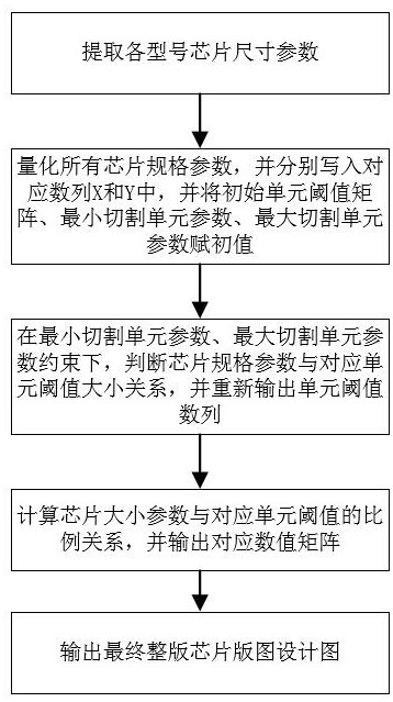
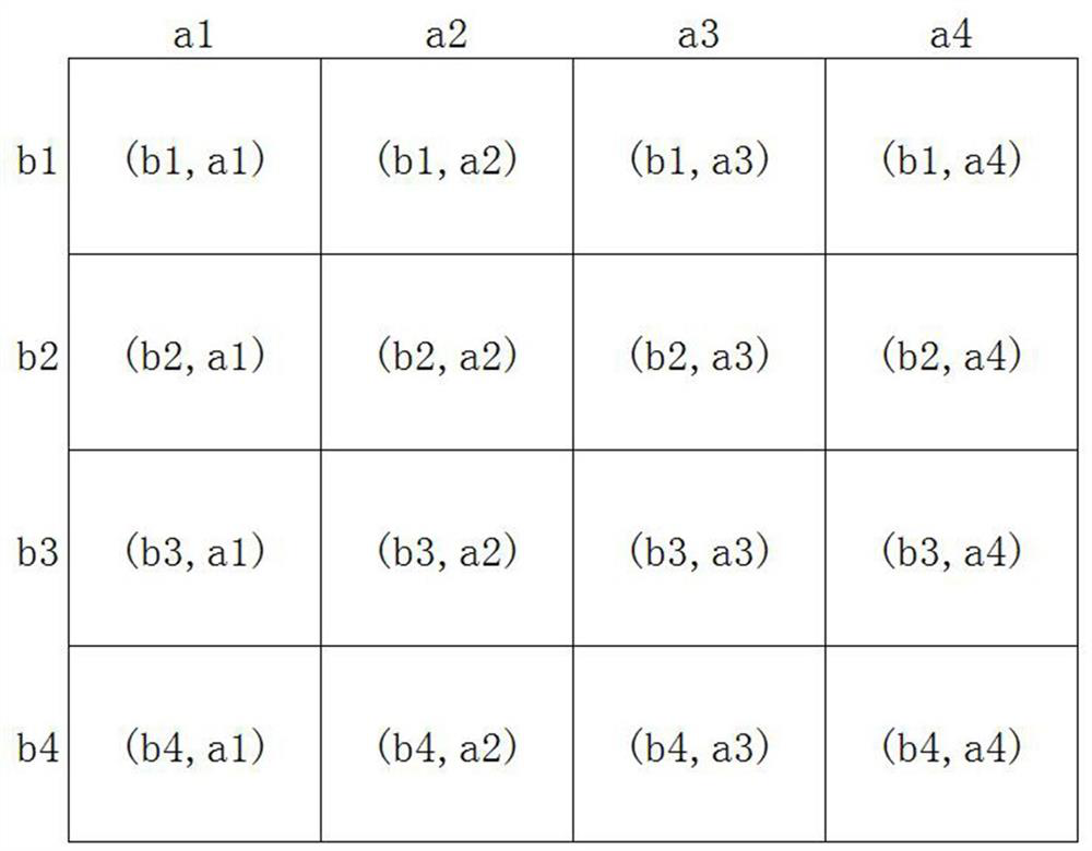
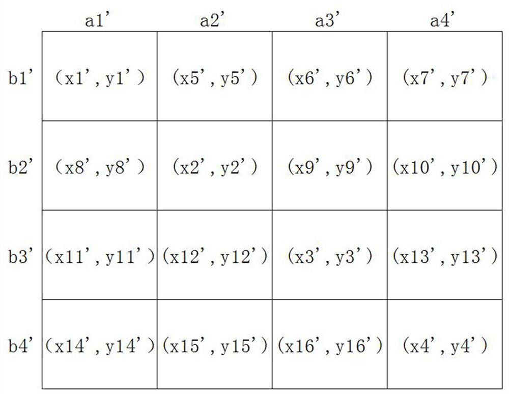
[0051] The technical solutions of the present invention will be clearly and completely described below with reference to the accompanying drawings. Obviously, the described embodiments are part of the embodiments of the present invention, but not all of the embodiments. Based on the embodiments of the present invention, all other embodiments obtained by those of ordinary skill in the art without creative efforts shall fall within the protection scope of the present invention.

[0052] In the description of the present invention, it should be noted that "center", "upper", "lower", "left", "right", "vertical", "horizontal", "inner", "outer", etc. The indicated direction or positional relationship is based on the direction or positional relationship described in the accompanying drawings, which is only for the convenience of describing the present invention and simplifying the description, rather than indicating or implying that the indicated device or element must have a specific...


PUM


Abstract

The invention discloses a layout design method of a multi-model chip and a chip and a terminal prepared by the layout design method, and belongs to the technical field of semiconductors, and the layout design method comprises the following steps: obtaining size parameters of each model of chip and initial values of each parameter quantity; under the constraint of the maximum cutting unit parameter and the minimum cutting unit parameter, the size relation between the chip size parameter and the corresponding initial unit threshold value is judged, and the chip unit threshold value is adjusted; and calculating a proportional relation between the threshold value of the corresponding chip unit and the chip size parameter, and outputting a layout design drawing. According to the method, the threshold values of the chip units are adjusted according to the sizes of the chips of different models, the whole layout can be quickly divided into a plurality of independent operation areas, then the proportional relation between the chips and the chip units is further calculated, the chips of the corresponding number are quickly arranged in the corresponding chip units, and in a certain threshold value range, the number of the chips is greatly reduced. The layout design can be simply, quickly and flexibly adjusted according to own chip design parameters of customers, and the layout design drawing is efficiently output.

Description

technical field [0001] The invention relates to the technical field of semiconductors, in particular to a layout design method of a multi-model chip and a chip and a terminal prepared therefrom. Background technique [0002] The layout design of integrated circuits plays a crucial role in the design process of silicon-based semiconductors, and is an important intermediate link in the circuit design and the driving process. Multi-customer wafer layout design is a routine business in the daily production of foundry companies. It is generally composed of multiple customers' tape-out requirements. There are various types of chips, and the number of requirements varies greatly. Under the premise of taking into account time efficiency and finished product yield, There is a certain difficulty in wafer layout design compatible with multiple customers. How to let layout design engineers quickly feedback the intuitive and accurate technical details about the final layout design requi...

Claims


Application Information

Patent Timeline
Patent Type & Authority Applications(China)
IPC IPC(8): G06F30/392H01L27/02G06F113/18
CPCG06F30/392H01L27/0207G06F2113/18Y02P90/30
Inventor 不公告发明人
Owner 成都复锦功率半导体技术发展有限公司
Why Eureka
Try Eureka