Semiconductor processing method and system

A processing method and semiconductor technology, applied in semiconductor/solid-state device manufacturing, manufacturing computing systems, electrical components, etc., can solve problems such as product quality impact, imperfect ingredients settings, etc., and achieve the effect of improving processing efficiency

Pending Publication Date: 2022-05-27
WUXI KUN CORE ELECTRONICS TECH CO LTD
View PDF4 Cites 0 Cited by
  • Summary
  • Abstract
  • Description
  • Claims
  • Application Information

AI Technical Summary

Problems solved by technology

[0003] In the process of semiconductor processing and production, it is necessary to set the ingredients according to the specific molding conditions of the semiconductor. After the ingredients are set, the semiconductor needs to be processed. Monitor the semiconductor manufacturing process. Usually, in semiconductor processing and manufacturing, due to the imperfect setting of ingredients in the processing process, it will affect the quality of semiconductor processed products.

Method used


Image

  • Semiconductor processing method and system
  • Semiconductor processing method and system

Examples


Embodiment 1

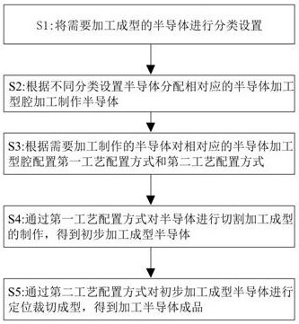
[0043] A semiconductor processing method, see figure 1 , the method includes the following steps:

[0044] S1: classify and set the semiconductors that need to be processed and formed;

[0045] S2: according to different classifications, semiconductor processing cavities corresponding to semiconductor allocation are set to process and manufacture semiconductors;

[0046] S3: configure the first process configuration mode and the second process configuration mode for the corresponding semiconductor processing cavity according to the semiconductor that needs to be processed and fabricated;

[0047] S4: by the first process configuration mode, the semiconductor is cut, processed and shaped to obtain a preliminary processing and shaped semiconductor;

[0048] S5: Positioning, cutting, and molding the preliminarily processed and formed semiconductor through the second process configuration to obtain a finished semiconductor product.

[0049] In the above process of manufacturing...

Embodiment 2

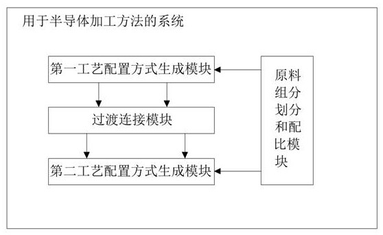
[0058] A system for a semiconductor processing method, see figure 2 , the system is used to realize the semiconductor processing method disclosed in Embodiment 1, and the advantages are that it is convenient for the processing and production of semiconductors, and improves the processing efficiency of semiconductors. ; Realize the connection between the first generation module and the second generation module through the structure used in the process of use

[0059] The second process configuration mode generates a module for processing the molded semiconductor;

[0060] a transition connection module, used for transferring the information of the first process configuration mode generation module to the second process configuration mode generation module;

[0061] The raw material component division and proportioning module is used to provide the detailed raw material component distribution ratio to the first process configuration mode module or the second process configurat...


PUM


Abstract

The invention discloses a semiconductor processing method and a semiconductor processing system, which are applied to the technical field of semiconductor processing, and are characterized in that the specific method comprises the following steps: performing classification setting on semiconductors needing to be processed and formed; arranging corresponding semiconductor processing cavities for processing and manufacturing the semiconductors according to different classifications of the semiconductors; configuring a first process configuration mode and a second process configuration mode for the corresponding semiconductor processing cavity according to the semiconductor needing to be processed and manufactured; cutting, processing and forming the semiconductor in the first process configuration mode to obtain a preliminarily processed and formed semiconductor; performing positioning, cutting and forming on the preliminarily processed and formed semiconductor in a second process configuration mode to obtain a processed semiconductor finished product; the method has the technical effects that the semiconductor is processed and manufactured by adopting a method of combining the first process configuration mode and the second process configuration mode, and the working efficiency is improved.

Description

technical field [0001] The present invention relates to the technical field of semiconductor processing, in particular to a semiconductor processing method and a system thereof. Background technique [0002] Semiconductors refer to materials with electrical conductivity between conductors and insulators at room temperature. Semiconductors are used in integrated circuits, consumer electronics, communication systems, photovoltaic power generation, lighting, high-power power conversion and other fields. Common diodes are made of semiconductors. Devices; no matter from the perspective of technology or economic development, the importance of semiconductors is very huge. Most electronic products, such as computers, mobile phones or digital recorders, the core units are very closely related to semiconductors. Related, common semiconductor materials are silicon, germanium, gallium arsenide, etc., silicon is the most influential one in the application of various semiconductor materia...

Claims


Application Information

Patent Timeline
IPC IPC(8): H01L21/67H01L21/02
CPCH01L21/67271H01L21/02Y02P90/30
Inventor 章泽润方敏
Owner WUXI KUN CORE ELECTRONICS TECH CO LTD
Why Eureka
Try Eureka