Defoaming type semiconductor chip packaging device

A packaging device and semiconductor technology, which is applied in the manufacture of semiconductor/solid-state devices, electrical components, circuits, etc., can solve the problems of cracking of epoxy resin layer, poor protection effect of electronic components, etc., and achieve the effect of improving the defoaming effect.

Pending Publication Date: 2022-05-31
郭中杰
View PDF0 Cites 2 Cited by
  • Summary
  • Abstract
  • Description
  • Claims
  • Application Information

AI Technical Summary

Problems solved by technology

[0003] In the prior art, epoxy resin is generally used for encapsulation, but when the epoxy resin is poured, there are often certain air bubbles inside, resulting in certain gaps in the formed epoxy resin layer, resulting in the actual use of the epoxy resin. Layers are prone to cracking, resulting in poor protection for internal electronic components

Method used


Image

  • Defoaming type semiconductor chip packaging device
  • Defoaming type semiconductor chip packaging device
  • Defoaming type semiconductor chip packaging device

Examples


Embodiment 1

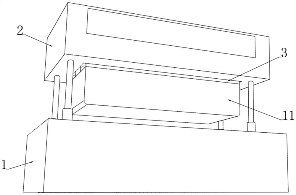
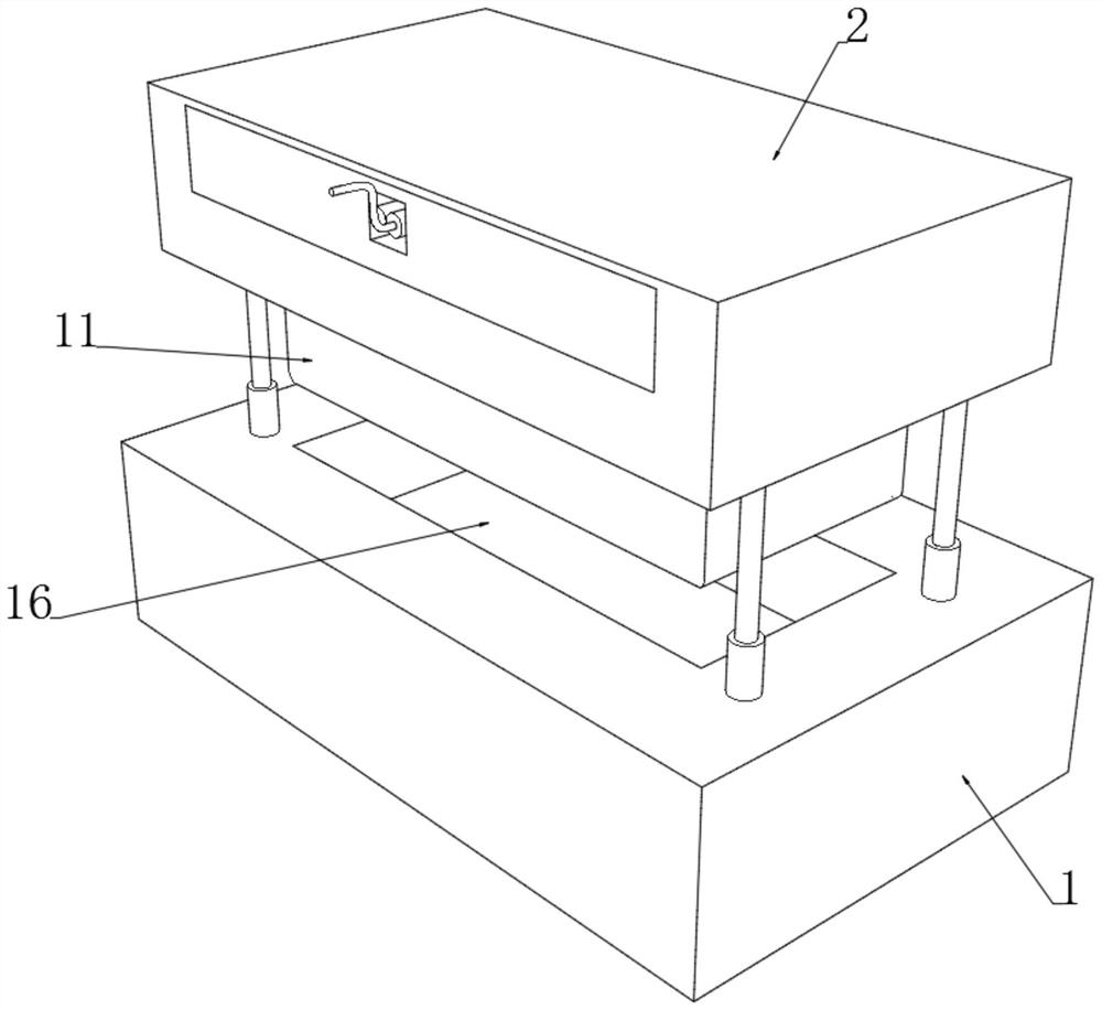
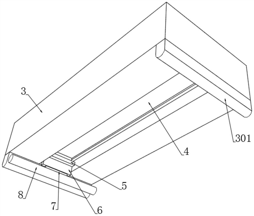
[0042] see Figure 1-4 , a defoaming type semiconductor chip packaging device, including a movable template 2 and a fixed template 1 arranged up and down, the fixed template 1 and the four corners of the movable template 2 are connected by hydraulic rods, and the upper end of the fixed template 1 is provided with a casting cavity , the bottom end of the movable template 2 is provided with an encapsulation seat 3 which is adapted to the pouring cavity, and both sides of the lower end of the encapsulation seat 3 are provided with elliptical guide seats 301. The electric sliding rail 4 is installed in the cavity, and the electric sliding rail 4 is connected with an intelligent lifting piece through the connecting plate 5. The bottom end of the intelligent lifting piece is connected with a magnetic bearing 8 that is flush with the bottom end surface of the oval guide seat 301. 3. The lower end is tightly covered with a flexible bag 11, and the bottom end wall of the flexible bag 1...


PUM


Abstract

The invention discloses a packaging device for a defoaming type semiconductor chip, and belongs to the field of chip packaging, a magnetic bearing capable of moving left and right and up and down and a flexible bag connected with the bottom end wall of the magnetic bearing in a wrapping manner are additionally arranged at the bottom end part of a packaging seat, and the flexible bag is extruded by means of horizontal and intermittent up and down movement of the magnetic bearing; after being extruded, the flexible bag presses a gap in the epoxy resin in the pouring cavity to be flat, meanwhile, an elastic packaging bottom film is additionally arranged at the bottom end of the pouring cavity, and a plurality of magnetic extrusion assisting components which are in magnetic attraction with the magnetic bearing are distributed at the lower end of the elastic packaging bottom film; the magnetic extrusion assisting component upwards extrudes the elastic packaging bottom film, so that the epoxy resin is extruded in a vertical horizontal wave shape, bubbles are effectively extruded from the bottom, the defoaming effect is comprehensively improved, and bubble holes in a packaging layer at the bottom end due to the fact that the bubbles remain at the bottom are effectively avoided.

Description

technical field [0001] The invention relates to the field of chip packaging, and more particularly, to a packaging device for defoaming semiconductor chips. Background technique [0002] Semiconductor packaging refers to the process of processing the tested wafer according to the product model and functional requirements to obtain an independent chip. The circuit pins on the silicon wafer are connected to external connectors with wires for connection with other devices. Packaging can also be used. Said to refer to the casing for installing semiconductor integrated circuit chips, it not only plays the role of placing, fixing, sealing, protecting the chip and enhancing thermal conductivity, but also a bridge to communicate the internal world of the chip and the external circuit - the wire for the contacts on the chip Connect to the pins of the package housing, which in turn establish connections to other devices through wires on the printed circuit board. [0003] In the prio...

Claims


Application Information

Patent Timeline
Patent Type & Authority Applications(China)
IPC IPC(8): B29C43/36B29C43/18H01L21/56
CPCB29C43/361B29C43/3642B29C43/18H01L21/565B29C2043/3647B29C2043/3652B29C2043/181
Inventor 郭中杰
Owner 郭中杰
Why Eureka
Try Eureka