Plasma processing apparatus
A plasma and processing device technology, applied in the field of plasma processing devices, can solve problems such as influence and substrate pollution to be processed, and achieve the effects of reducing particle pollution, improving etching uniformity, and being less prone to particle pollution
- Summary
- Abstract
- Description
- Claims
- Application Information
AI Technical Summary
Problems solved by technology
Method used
Image

Examples
Embodiment Construction
[0021] As described in the background art, the particle contamination of the substrate to be processed is relatively serious in the existing plasma processing apparatus. Therefore, the present invention aims to provide a plasma processing apparatus to reduce the particle contamination of the substrate to be processed and ensure the The smoothness of the transmission path is described in detail as follows:
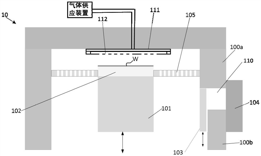
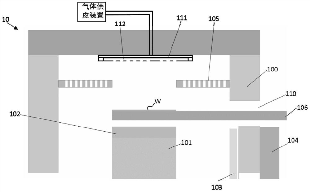
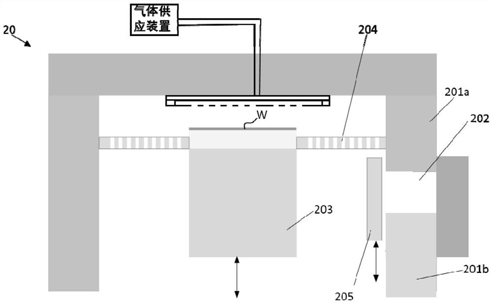
[0022] figure 1 It is a schematic structural diagram of a plasma processing device of the present invention.
[0023] Please refer to figure 1 , the plasma processing apparatus 1 includes: a reaction chamber, which includes a side wall of the reaction chamber, the side wall of the reaction chamber has a substrate transfer port 110, and the substrate transfer port 110 has a first distance from the bottom of the reaction chamber; movable The lower electrode assembly 101 is arranged at the bottom of the reaction chamber, and is used to carry the substrate W to be processed; ...
PUM
 Abstract
Description
Claims
Application Information
 - R&D
- Intellectual Property
- Life Sciences
- Materials
- Tech Scout
- Unparalleled Data Quality
- Higher Quality Content
- 60% Fewer Hallucinations
Browse by: Latest US Patents, China's latest patents, Technical Efficacy Thesaurus, Application Domain, Technology Topic, Popular Technical Reports.
© 2025 PatSnap. All rights reserved.Legal|Privacy policy|Modern Slavery Act Transparency Statement|Sitemap|About US| Contact US: help@patsnap.com