
Dynamic D flip-flop for improving pseudo static loop based on negative feedback

A negative feedback, flip-flop technology, applied in pulse technology, pulse generation, electrical components, etc., can solve the problems of D flip-flop function failure, data cannot be written, etc., to ensure high-speed advantages, ensure functions, and improve data writing. Effect

Pending Publication Date: 2022-05-31
BEIJING UNIV OF TECH
View PDF0 Cites 0 Cited by
  • Summary
  • Abstract
  • Description
  • Claims
  • Application Information

AI Technical Summary

Problems solved by technology

If the size of the pseudo-static loop is too large, different data cannot be written into the D flip-flop, thereby invalidating the function of the D flip-flop

Method used


Image

  • Dynamic D flip-flop for improving pseudo static loop based on negative feedback
  • Dynamic D flip-flop for improving pseudo static loop based on negative feedback
  • Dynamic D flip-flop for improving pseudo static loop based on negative feedback

Examples


specific Embodiment 1

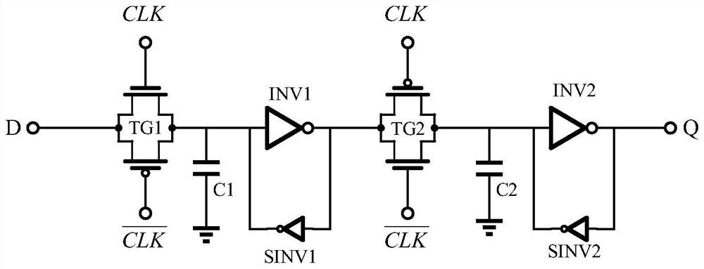
[0031] Combine the following figure 2 The specific circuit connections and implementations and device parameters of the present invention are described.

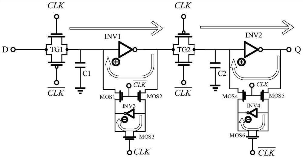
[0032] In order to solve the pseudo-static loop problem of the dynamic D flip-flop, the present invention proposes a circuit based on sequential control and negative feedback control. The entire circuit consists of transmission gates, charge storage, inverters and MOS transistors. figure 2 The first stored charge C1 and the second stored charge C2 are replaced by the parasitic capacitances of the gates in the input stages of the first inverter INV1 and the second INV2. Using the parasitic capacitance as a capacitor for storing charges can reduce the data writing time on the one hand and the layout area on the other hand.

[0033] The connection relationship of the specific embodiment 1 is as follows: the first transmission gate TG1, one end is connected to the input signal D, and the other end is connected to the input e...

Embodiment 2

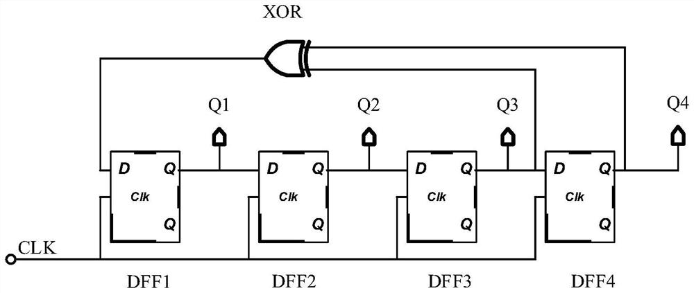
[0045] image 3 The middle is the logic structure diagram of pseudo-random sequence generation, in which the input D terminal and output Q terminal of the first D flip-flop DFF1, the second D flip-flop DFF2, the third D flip-flop DFF3, and the fourth D flip-flop DFF4 are cascaded , that is, the output Q1 terminal of the first D flip-flop DFF1 is connected to the input D2 terminal of the second D flip-flop DFF2, the output Q2 terminal of the second D flip-flop DFF2 is connected to the input D3 terminal of the third D flip-flop DFF3, and the third The output Q3 terminal of the D flip-flop DFF3 is connected to the input D4 terminal of the fourth D flip-flop DFF4, and the output Q3 terminal of the third D flip-flop DFF1 and the output Q4 terminal of the fourth flip-flop DFF4 are connected to the XOR of the exclusive OR gate in the figure. The input terminal is used for XOR operation, and the output terminal of the XOR gate XOR is connected to the input terminal of the first flip-flo...

Embodiment 3

[0048] Figure 4 In the middle is a two-frequency divider formed by using the dynamic D flip-flop of the present invention. The clock terminal of the first D flip-flop DFF1 is connected to the first forward clock CLK, the output Q1 terminal is connected to the input terminal of the first inverter INV1 and the input terminal of the second inverter INV2, and the output of the first inverter INV1 The terminal is connected to the input D1 terminal of the first D flip-flop, and the output terminal of the second inverter INV2 is to output the divided-by-2 frequency signal OUT of the first forward clock CLK.

[0049] The frequency dividing buffer stage of the second inverter INV2 improves the driving capability of the frequency dividing. Figure 7 The time domain waveform of the frequency divider formed by the improved dynamic D flip-flop structure based on the negative feedback pseudo-static loop is shown. Input a high-frequency 5GHz clock signal, and the output is a 2.5GHz divide...


PUM


Abstract

The invention relates to a dynamic D flip-flop for improving a pseudo static loop based on negative feedback. A traditional dynamic D trigger uses charges to store data information, so that the charges discharge through a resistor under a low-frequency clock to cause data loss. According to traditional optimization, a small-size inverter is added to charge and discharge a capacitor to keep data stable. However, two stages of phase inverters are cascaded to form a positive feedback register structure, and when data are changed, stronger write-in capability or longer write-in time is needed. According to the structure provided by the invention, through sequential control, when data is written in, the pseudo static loop is disconnected from the main circuit, and self-discharging or self-charging is performed in advance through negative feedback, so that the transmission delay of the data is reduced. And when the data is kept, the pseudo static loop is connected with the main circuit to keep the data stable. According to the invention, the stability of low-frequency data is ensured without influencing the high-frequency characteristic of the dynamic D flip-flop.

Description

technical field [0001] The invention relates to a dynamic D flip-flop for improving pseudo-static loop based on negative feedback. Background technique [0002] The traditional CMOS dynamic D flip-flop is different from the CMOS static D flip-flop. The CMOS static D flip-flop requires 4 inverters and 4 transmission gates, while the dynamic D flip-flop maintains data by increasing the input stage capacitor to store charge. However, if the data input by the next beat clock is different from the stored data, it is very likely to charge and discharge the input stage capacitor, resulting in bit errors. To solve the problem of the instability of its stored charge, the traditional method maintains the charge by adding a pseudo-static loop. like figure 1 As shown, a register structure is formed by adding a small-sized inverter and the inverter in the dynamic D flip-flop. The design of the pseudo-static loop greatly improves the anti-noise performance of the storage node, which es...

Claims


Application Information

Patent Timeline
IPC IPC(8): H03K3/356
CPCH03K3/356104
Inventor 刘素娟刘堃葛傲冉
Owner BEIJING UNIV OF TECH
Learn More