Wafer bonding magnetic alignment method and device

A wafer bonding and alignment device technology, applied in transportation and packaging, semiconductor devices, electrical components, etc., can solve problems such as calibration errors, unsure alignment, errors, etc., to reduce errors, improve efficiency and alignment Accurate accuracy, the effect of improving efficiency

Pending Publication Date: 2022-06-17
BEIJING UNIV OF TECH
View PDF1 Cites 0 Cited by
  • Summary
  • Abstract
  • Description
  • Claims
  • Application Information

AI Technical Summary

Problems solved by technology

This will cause calibration errors, and after alignment, it needs to go through a large stroke of movemen

Method used


Image

  • Wafer bonding magnetic alignment method and device
  • Wafer bonding magnetic alignment method and device
  • Wafer bonding magnetic alignment method and device

Examples


Example Embodiment

[0035]为使本发明实施例的目的、技术方案和优点更加清楚,下面将结合本发明实施例的附图,对本发明实施例的技术方案进行清楚、完整地描述。所举实例只用于解释本发明,并非用于限定本发明的范围。

[0036]下面结合附图具体描述根据本发明实施例的晶圆键合磁对准方法及装置。如图7至图8所示,根据本发明实例的晶圆键合磁对准装置具体包括:X-Y移动系统1,底部晶圆键合台5,磁传感器模块7,键合臂模块17,装置底座及框架22。

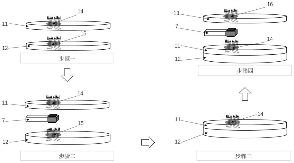
[0037]具体地,本发明的一种实施例中的晶圆键合磁对准方法工作流程参见图1,图中仅示意一处对准标记的对准方法及原理,其他对准标记使用相同方式对准。由图1中所示,对准步骤主要分为四个步骤:

[0038]步骤一:先利用X-Y移动系统1将已经拾取下晶圆12的底部晶圆键合台5移动至预先设定好的位置处,同时键合臂模块17中的键合头18也同时拾取上晶圆11,此时还未开始对准。步骤二:在本实施例中,将磁传感器模块7设在上晶圆11与下晶圆12中间并分布在两侧,利用两个磁传感器8夹头分别夹住上下不同的磁传感器8,先利用上部磁传感器8检测上晶圆11中的晶圆对准标记位置信息,把获取的位置信息采集并记录下。再通过下部磁传感器8检测下晶圆12中的晶圆对准标记位置信息,由于上晶圆11与下晶圆12的位置差异,利用X-Y移动系统1进行粗对准,再通过精对准微纳米平台4实现高精度对准。步骤三:对准完成后,通过键合臂模块17进行键合运动,实现上晶圆11与下晶圆12之间的键合。步骤四:图中所示为继续重复步骤二的对准方式进行第n层晶圆13的对准,同时继续检测n层晶圆对准标记16的位置信息,完成对准及键合。本实施例的优势在于可检测上一次对准后的键合精度,并根据键合后的位置误差进行反馈和调整下一次键合。

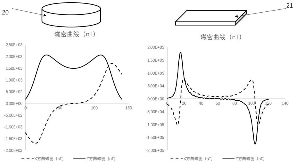
[0039]参见图5和图3,为本发明中对准标记空间磁场曲线图和晶圆对准装置的一种对准实施例。

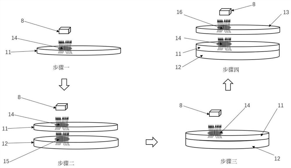
[0040]其对准方法布置方式如图5所示,上晶圆11已通过传输模块传输到键合臂模块17中的键合头18上,底部晶圆键合台5也已拾取传输过来的下晶圆12,此时上下晶圆12已经通过X-Y移动系统1移动到预先设计好的位置,此时还未进行对准,同时磁传感器模块7在垂直方向设在上晶圆11与下晶圆12之间,水平方向设在其两侧,为晶圆对准提供准备。

[0041]进一步地,本实施例中的对准原理及其对准标记参见图3所示。其中列举了两种...


PUM


Abstract

The invention discloses a wafer bonding magnetic alignment method and device. The device at least comprises an X-Y moving system, a bottom wafer bonding table, a magnetic sensor module, a bonding arm module, a device base and a frame. According to the method, counterpoint grooves are formed in a wafer through a semiconductor processing technology, magnetic columns made of magnetic materials are deposited in the grooves, and the magnetic columns have the permanent magnet characteristic after being magnetized. The space magnetic field distribution in the magnetic column of the wafer is detected through the magnetic sensor, and the boundary or the center of the magnetic column is found, so that the position information of the wafer is detected. Compared with a traditional optical alignment mode, the magnetic sensor does not need to calibrate the position, alignment is carried out when the distance between the two wafers is in the micron order, movement alignment and direct bonding are not needed after alignment, and the wafer bonding efficiency and precision are improved.

Description

technical field [0001] The invention relates to the technical field of semiconductors, in particular to a method and device for magnetic alignment of wafer bonding. Background technique [0002] In recent years, the integrated circuit industry has developed rapidly, and the demand for semiconductor chip functions has continued to increase. The integrated circuit industry is of great significance to my country's economic development. But Moore's Law has reached the physical limit, and the existing solutions are developing from 2D plane to 3D integration, continuing Moore's Law. Wafer-level bonding is a particularly important link in 3D integration technology. The alignment technology in wafer bonding is closely related to the performance of the produced chips. With the continuous progress and development of semiconductor technology, the accuracy of the marking lines on the wafer is getting higher and higher. High-quality alignment accuracy can avoid alignment patterns. Prob...

Claims


Application Information

Patent Timeline
IPC IPC(8): H01L21/67H01L21/677H01L21/68
CPCH01L24/83H01L21/67259H01L21/68H01L21/6776H01L2224/832
Inventor 叶乐志宋宣颉常悦
Owner BEIJING UNIV OF TECH
Why Eureka
Try Eureka