Three-dimensional chip layout method and device and terminal equipment

A three-dimensional chip and layout method technology, applied in the computer field, can solve the problems of low layout accuracy and increase power consumption of three-dimensional chips, and achieve the effects of improving layout accuracy, prolonging service life and reducing power consumption

Pending Publication Date: 2022-07-01
CHINA GREATWALL TECH GRP CO LTD
View PDF0 Cites 2 Cited by
  • Summary
  • Abstract
  • Description
  • Claims
  • Application Information

AI Technical Summary

Problems solved by technology

[0004] The embodiment of the present application provides a layout method, device, terminal equipment and computer-readable storage medium for a three-dimensional chip, which can solve the problems of low layout accuracy and increased power consumption of the three-dimensional chip in the prior art

Method used


Image

  • Three-dimensional chip layout method and device and terminal equipment
  • Three-dimensional chip layout method and device and terminal equipment
  • Three-dimensional chip layout method and device and terminal equipment

Examples


Embodiment Construction

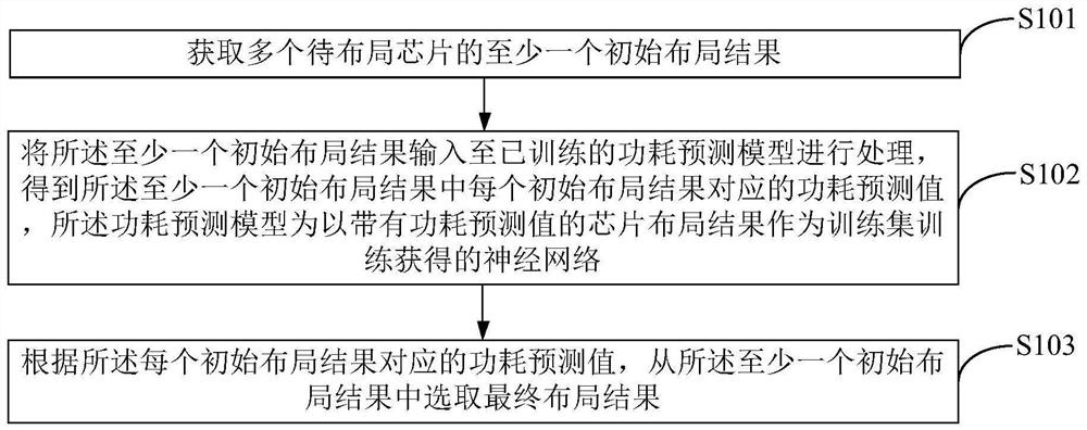
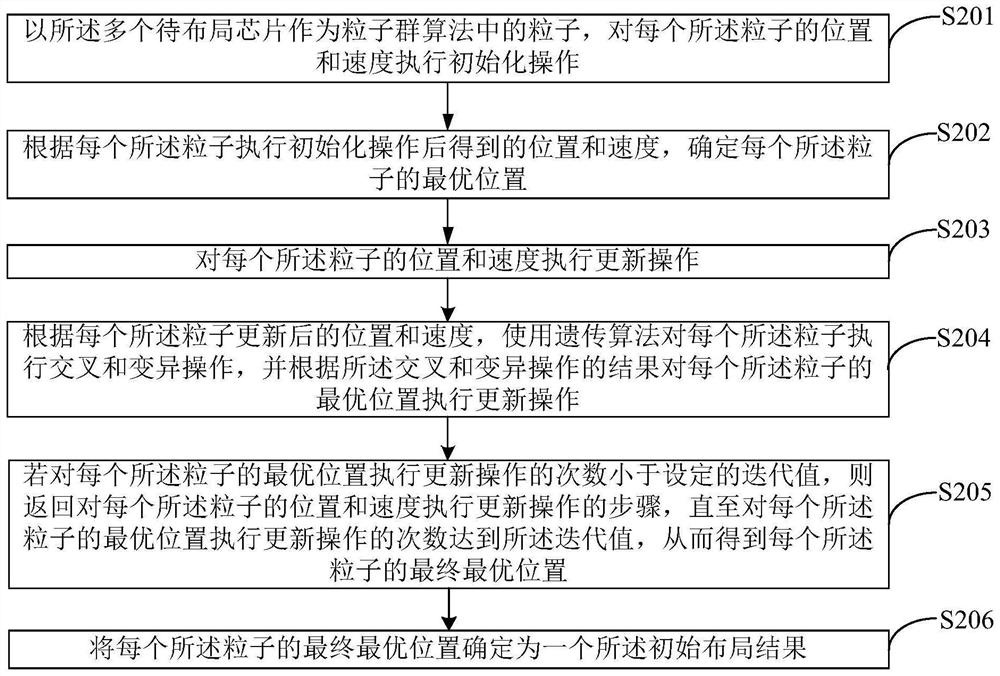
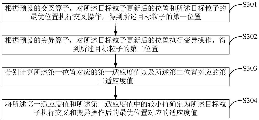
[0052] In the following description, for the purpose of illustration rather than limitation, specific details, such as specific system structures and technologies, are provided for a thorough understanding of the embodiments of the present application. However, it will be apparent to those skilled in the art that the present application may be practiced in other embodiments without these specific details. In other instances, detailed descriptions of well-known systems, devices, circuits, and methods are omitted so as not to obscure the description of the present application with unnecessary detail.

[0053] It is to be understood that, when used in this specification and the appended claims, the term "comprising" indicates the presence of the described feature, integer, step, operation, element and / or component, but does not exclude one or more other The presence or addition of features, integers, steps, operations, elements, components and / or sets thereof.

[0054] It will a...


PUM


Abstract

The invention is suitable for the technical field of computers, and provides a three-dimensional chip layout method and device and terminal equipment, and the method comprises the steps: obtaining at least one initial layout result of a plurality of chips to be laid out; the at least one initial layout result is input into a trained power consumption prediction model for processing, a power consumption prediction value corresponding to each initial layout result in the at least one initial layout result is obtained, and the power consumption prediction model is a neural network obtained by taking the chip layout result with the power consumption prediction value as a training set for training; and selecting a final layout result from the at least one initial layout result according to the power consumption predicted value corresponding to each initial layout result. According to the three-dimensional chip layout method provided by the invention, the influence of power consumption on the three-dimensional chip layout is considered, the layout accuracy of the three-dimensional chip is improved, the power consumption of the three-dimensional chip is reduced, and the service life of the three-dimensional chip is further prolonged.

Description

technical field [0001] The present application belongs to the field of computer technology, and in particular, relates to a three-dimensional chip layout method, device, terminal device, and computer-readable storage medium. Background technique [0002] In recent years, with the wide application of three-dimensional packaging technology, the integration and complexity of chips have been increasing. The number of components integrated in a chip has continued to increase and the density has continued to increase. getting bigger. Compared with the conventional two-dimensional integrated chip, the three-dimensional stacked chip of the same area can integrate more chips, which greatly increases the power per unit volume, and easily causes the problem of overheating or even failure of the stacked chip. Therefore, how to layout the three-dimensional chip has become one of the key issues in the automation of integrated circuit electronic design. [0003] However, the prior art us...

Claims


Application Information

Patent Timeline
Patent Type & Authority Applications(China)
IPC IPC(8): G06F30/392G06F30/398
CPCG06F30/392G06F30/398
Inventor 涂宏斌刘雨芃赵瑞敏徐学明徐任玉
Owner CHINA GREATWALL TECH GRP CO LTD
Why Eureka
Try Eureka