Chip packaging method and chip module

A technology of chip module and packaging method, which is applied in the direction of semiconductor/solid-state device parts, semiconductor devices, electrical components, etc., can solve the problems of increasing manufacturing time and cost, fatigue fracture of thin gold wire materials, cumbersome process, etc., and achieve reduction The effect of manufacturing time and cost

Pending Publication Date: 2022-07-01
INST OF FLEXIBLE ELECTRONICS TECH OF THU ZHEJIANG +1
View PDF0 Cites 0 Cited by
  • Summary
  • Abstract
  • Description
  • Claims
  • Application Information

AI Technical Summary

Problems solved by technology

However, in the actual use environment, since the thin gold wire material itself is prone to fatigue and fracture under bending, it is difficult to break through such technical problems only from the material of the gold wire itself.
Therefore, there are certain problems in the stability and reliability of this process product.
Moreover, the interconnection process using gold wires is relatively cumbersome. It is necessary to bond the flexible chip on the substrate first, and then electrically connect the pads on the flexible chip to the pads on the substrate one by one through gold wires, increasing the manufacturing time and cost

Method used


Image

  • Chip packaging method and chip module
  • Chip packaging method and chip module
  • Chip packaging method and chip module

Examples


Embodiment Construction

[0025] In order to further illustrate the technical means and effects adopted by the present invention to achieve the predetermined purpose of the invention, the following describes the specific implementation, structure, Features and their efficacy, detailed as follows:

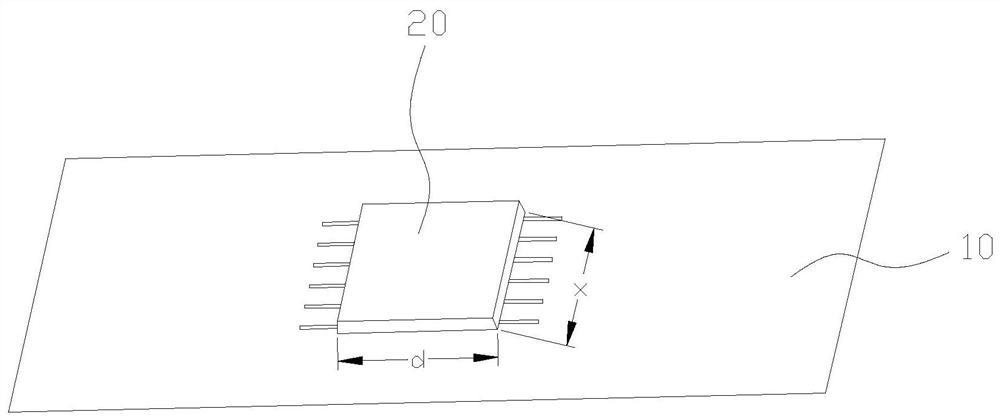
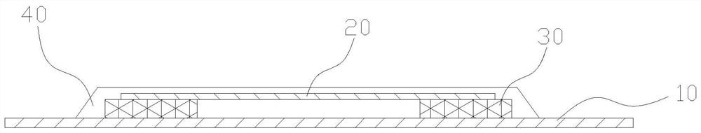
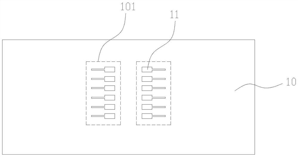
[0026] figure 1 is the three-dimensional structural schematic diagram of the chip module in the present invention, figure 2 is a schematic diagram of the cross-sectional structure of the chip module in the present invention, image 3 is the top-view structural schematic diagram of the substrate in the present invention, Figure 4 It is a top-view structural schematic diagram of the substrate and the conductive rubber strip in the present invention, Figure 5 It is a schematic diagram of the three-dimensional structure of the conductive rubber strip in one of the embodiments of the present invention, Image 6 It is a schematic diagram of the three-dimensional structure of the conductive rubber strip in a...


PUM

PropertyMeasurementUnit
thicknessaaaaaaaaaa
electrical resistivityaaaaaaaaaa

Abstract

The invention discloses a chip packaging method and a chip module, the chip module comprises a substrate, a chip and a conductive adhesive tape arranged between the substrate and the chip, the substrate is provided with a plurality of first bonding pads, the chip is provided with a plurality of second bonding pads, and the conductive adhesive tape is used for conductively connecting the second bonding pads with the first bonding pads corresponding to the second bonding pads respectively. The conductive adhesive tape comprises a plurality of conductive layers and a plurality of insulating layers, the conductive layers and the insulating layers are alternately stacked in the arrangement direction of the first bonding pads, one conductive layer corresponds to one first bonding pad and one second bonding pad at most, and one first bonding pad and one second bonding pad correspond to at least one conductive layer. The first bonding pad on the substrate and the second bonding pad on the chip are conductively connected through the conductive adhesive tape, the first bonding pad on the substrate and the second bonding pad on the chip do not need to be electrically connected one by one through a gold wire, the manufacturing time and cost are reduced, and the conductive adhesive tape is flexible and cannot be subjected to fatigue fracture when bent.

Description

technical field [0001] The invention relates to the technical field of chip packaging, in particular to a chip packaging method and a chip module. Background technique [0002] Traditional semiconductors use plastic packaging, ceramic packaging and metal packaging. These packaging methods are all rigid packaging and cannot be flexible, which restricts the form of electronic products. In the general packaging process of flexible chips, the chip is bonded to the substrate on the front side by die attach adhesive (DAF, dieattach film, wafer adhesive film), and is interconnected by gold wires to connect the solder joints of the chip and the solder joints of the substrate. At present, the development of flexible electronic technology adopts wafer thinning and flexible substrate bonding, and uses gold wire interconnection to realize the process technology of stable operation of semiconductor chips under a certain curvature radius. However, in the actual use environment, since the...

Claims


Application Information

Patent Timeline
Patent Type & Authority Applications(China)
IPC IPC(8): H01L23/49H01L21/60
CPCH01L23/49H01L24/85H01L24/45H01L2224/45005H01L2224/4503H01L2224/4502H01L2224/8538
Inventor 葛沈浩
Owner INST OF FLEXIBLE ELECTRONICS TECH OF THU ZHEJIANG
Why Eureka
Try Eureka