Chip packaging structure

A chip packaging structure and chip technology, applied in the direction of semiconductor/solid-state device components, semiconductor devices, electrical components, etc., can solve the problems of chip temperature rise, size limitation, inapplicability, etc.

Pending Publication Date: 2022-07-01
RICHTEK TECH
View PDF2 Cites 0 Cited by
  • Summary
  • Abstract
  • Description
  • Claims
  • Application Information

AI Technical Summary

Problems solved by technology

However, this design has several disadvantages: 1. The space between the outer cover 220 and the chip will accumulate waste heat, causing the temperature of the chip CH to rise
2. The outer cover 220 is made by another process, and its size is limited due to the manufacturing, so it is not suitable for small-sized chip packaging

Method used


Image

  • Chip packaging structure
  • Chip packaging structure
  • Chip packaging structure

Examples


Embodiment Construction

[0038] The drawings in the present invention are schematic, mainly intended to show the relationship between the components of the various elements, and the shapes and sizes are not drawn according to scale.

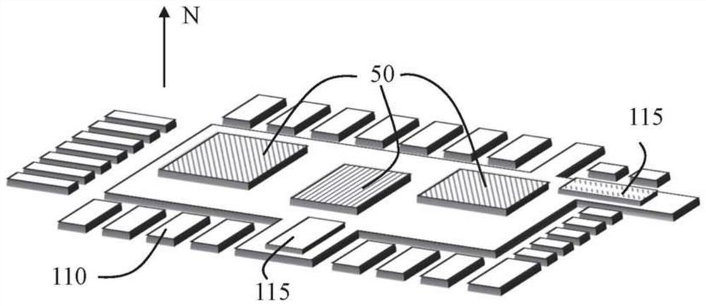
[0039] In order to provide high-efficiency heat dissipation function, according to one point of view, refer to Figure 3A and Figure 3B , Figure 3A It is a schematic diagram of the state before encapsulation, Figure 3B Schematic diagram of the state after encapsulation of the encapsulation material. Among them, the present invention provides a chip package structure 10, which includes: at least one semiconductor chip 50, which has a signal processing function, and optionally has at least one copper pillar 55 (Copper pillar). The number of copper pillars 55 of the present invention is not limited to this number, and it can be determined according to the needs of heat dissipation, such as no copper pillars, one or more copper pillars; a substrate 110, and the semicon...


PUM


Abstract

A chip package structure includes: at least one semiconductor chip having a signal processing function; a substrate, wherein the semiconductor chip is arranged on the substrate; the at least one heat transfer patch is arranged on the substrate; and an encapsulation material encapsulating the substrate, the heat transfer patch and the semiconductor chip, in which the heat transfer patch forms at least one heat transfer path.

Description

technical field [0001] The invention relates to a chip packaging structure, in particular to a chip packaging structure in which a heat transfer patch and / or a copper post are attached to a substrate to enhance the heat transfer effect. Background technique [0002] In the prior art, refer to figure 1 , which shows the chip package structure of the Korean patent case KR 101271374, and the substrate 110 is made of a silicon material. For heat conduction effect, many grooves 220 are arranged on the substrate to increase the heat dissipation area. This production process needs to go through processes such as photomask corrosion, and the production is complicated. In addition, the heat to be removed is easily accumulated in the groove 220, and the heat dissipation effect is limited. [0003] refer to figure 2 , which shows the chip package structure of US Patent No. 8,202,765. figure 2 The middle chip CH is connected to the outer cover 210 via the thermally conductive mat...

Claims


Application Information

Patent Timeline
Patent Type & Authority Applications(China)
IPC IPC(8): H01L25/18H01L23/367H01L23/495
CPCH01L25/18H01L23/3677H01L23/49568H01L23/4334H01L23/49541H01L23/49575H01L2224/16225H01L2224/73253H01L23/3107H01L23/3114H01L23/367H01L23/49513H01L23/15
Inventor 林士杰胡永中黄恒赍颜豪疄
Owner RICHTEK TECH
Why Eureka
Try Eureka