Printed board crystal supplementing and repairing device

A printed circuit board and rework technology, applied in the direction of printed circuit manufacturing, printed circuit, printed circuit secondary treatment, etc., can solve the problems of increased production process, many processes, increased cost, etc., to reduce product yield and reduce production process , the effect of improving work efficiency

Pending Publication Date: 2022-07-01
深圳市易天半导体设备有限公司
View PDF0 Cites 3 Cited by
  • Summary
  • Abstract
  • Description
  • Claims
  • Application Information

AI Technical Summary

Problems solved by technology

At present, in order to solve this problem, it is usually necessary to use multiple separate equipment, which will inevitably lead to an increase in the product...

Method used


Image

  • Printed board crystal supplementing and repairing device
  • Printed board crystal supplementing and repairing device
  • Printed board crystal supplementing and repairing device

Examples


Embodiment Construction

[0049] In order to make those skilled in the art better understand the solution of the present invention, the present invention is further described in detail below with reference to the accompanying drawings and embodiments.

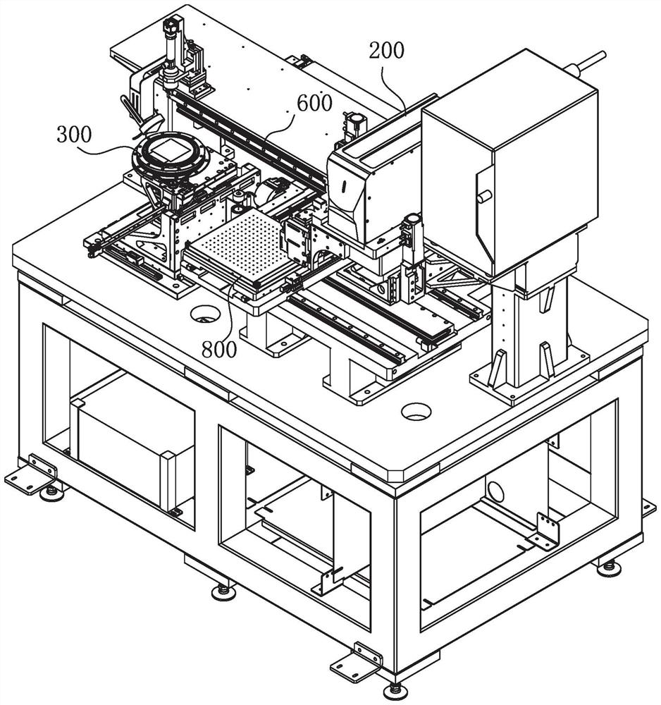
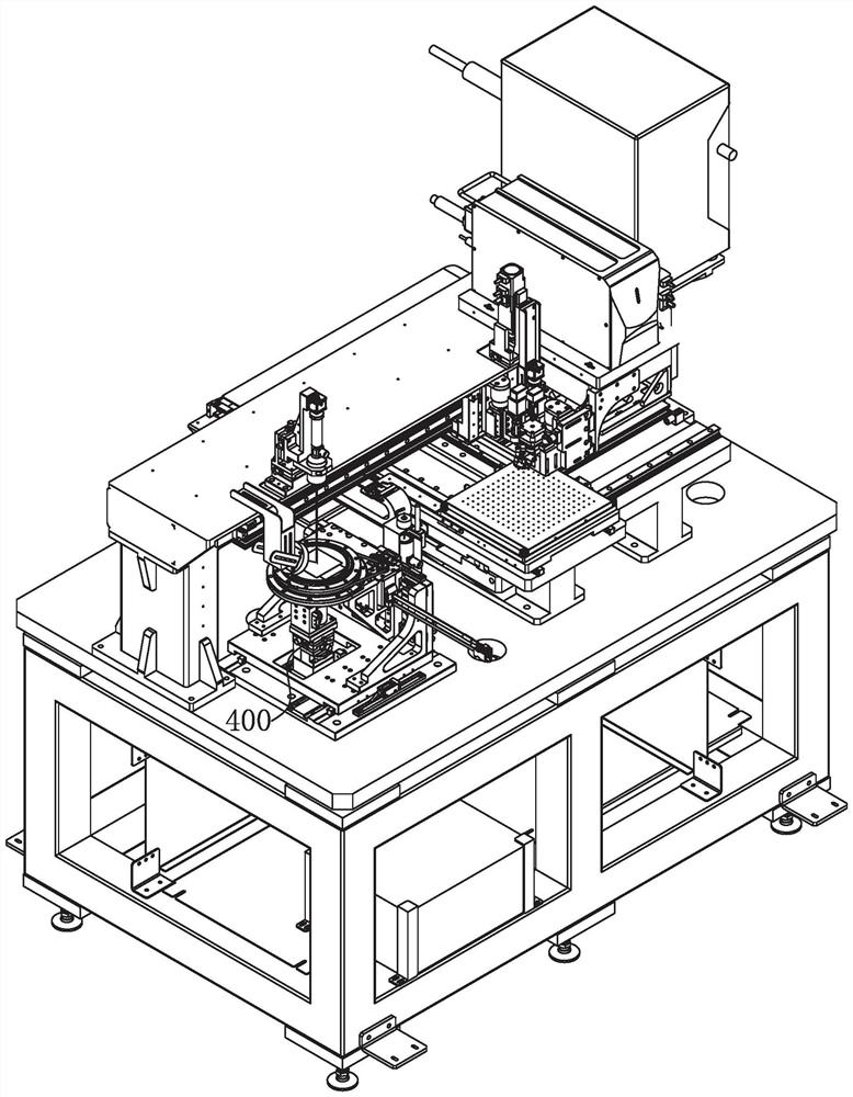
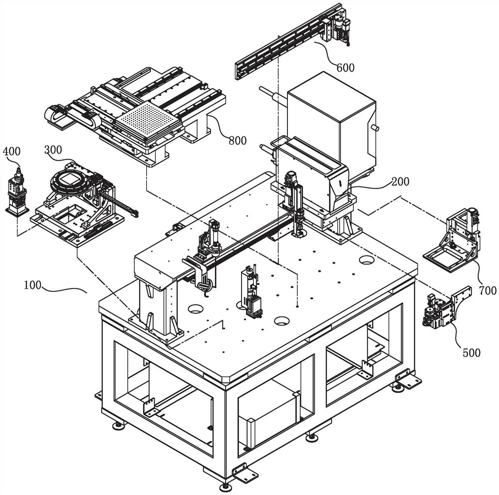
[0050] like Figure 1-3 As shown, an embodiment of the present invention provides a device for patching and repairing printed circuit boards, including a frame 100, and further comprising: a laser module 200 disposed on the frame; the laser module here is a commercially available standard part, namely Laser; film module 300, which is installed on the rack 100 for moving the blue film chip tray on which the chip is placed; needle module 400, which is installed on the rack 100 and is located below the blue film chip disk , used to impact the chip placed on the blue film chip tray; the dispensing module 500, which is arranged on the rack 100, is used to apply solder paste on the printed board where the chip needs to be filled; the nozzle module 600 , whic...


PUM


Abstract

The invention belongs to the technical field of semiconductor processing equipment, and particularly relates to a printed board crystal supplementing and repairing device which comprises a rack and further comprises a laser module arranged on the rack. The film module is used for moving a blue film chip disc which is arranged on the film module and is used for placing chips; the needle module is located below the blue film chip disc and used for impacting the chips placed on the blue film chip disc; the dispensing module is used for smearing solder paste on the position, where the chip needs to be complemented, of the printed board; the suction nozzle module is used for sucking the chips on the blue film chip disc and placing the chips on the solder paste-coated bonding pad on the printed board; the pressing module is used for fixing the to-be-welded chip placed on the printed board; and the transfer module is used for moving the printed board to the stations where the dispensing module, the suction nozzle module, the pressing module and the laser module are located. Compared with the prior art, the chip repairing and repairing device integrates chip repairing and welding processes on one device, so that the production process is effectively reduced, the operation efficiency and the product yield are improved, and the occupied area is reduced.

Description

technical field [0001] The invention relates to the technical field of semiconductor processing equipment, in particular to a device for supplementing chips for vacancies on a printed board. Background technique [0002] In the production process of the circuit board, the phenomenon of leakage and bad crystal is inevitable, that is, the chip is not placed in a certain position on the printed board where the chip needs to be placed. At present, in order to solve this problem, it is usually necessary to use multiple separate equipment to complete, which will inevitably lead to increased production processes, many processes, low product yield and efficiency, and requires more space to install processing equipment, resulting in a substantial increase in cost. SUMMARY OF THE INVENTION [0003] In order to overcome the deficiencies of the prior art, the purpose of the present invention is to provide a device for repairing and repairing a printed board, which aims to solve the pr...

Claims


Application Information

Patent Timeline
IPC IPC(8): H05K3/22H05K3/34H05K3/00
CPCH05K3/225H05K3/34H05K3/0008H05K2203/107H05K2203/17
Inventor 黄招凤陈罡彪游燚陈学志
Owner 深圳市易天半导体设备有限公司
Why Eureka
Try Eureka