LED packaging structure and display panel
A technology of LED packaging and LED chips, which is applied in the direction of semiconductor devices, electrical components, circuits, etc., can solve the problems of high blue light content, low luminous efficiency, and low power, and achieve the effect of improving luminous efficiency and reducing blue light components
- Summary
- Abstract
- Description
- Claims
- Application Information
AI Technical Summary
Problems solved by technology
Method used
Image
Examples
Embodiment 1
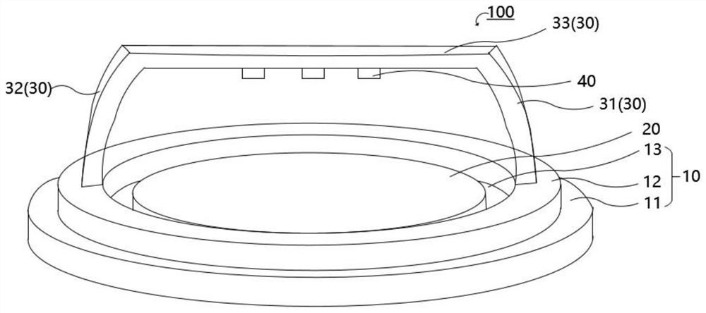
[0029] see figure 1 , figure 1 This is a first three-dimensional structural schematic diagram of an LED package structure 100 provided in an embodiment of the present application.
[0030] The embodiment of the present application provides an LED package structure 100 , and the LED package structure 100 includes a housing 10 , a quantum dot layer 20 , a bracket 30 , and an LED chip 40 . The housing 10 includes a bottom plate 11 and a side wall 12 arranged on the bottom plate 11, the bottom plate 11 and the side wall 12 form a groove 13; the quantum dot layer 20 is arranged on the bottom plate 11 in the groove 13; the bracket 30 is arranged above the groove 13 ; The LED chip 40 is arranged on the side surface of the bracket 30 facing the groove 13 , and the light-emitting direction of the LED chip 40 faces the quantum dot layer 20 .
[0031] Specifically, the housing 10 includes a bottom plate 11 and a side wall 12 disposed on the bottom plate 11 . The bottom plate 11 and the...
Embodiment 2
[0042] This embodiment is the same as or similar to the above-mentioned embodiment, and the difference lies in that the features of the LED package structure are further described.
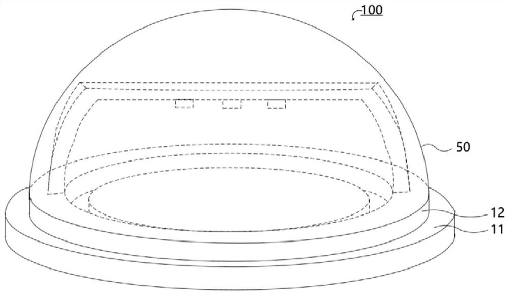
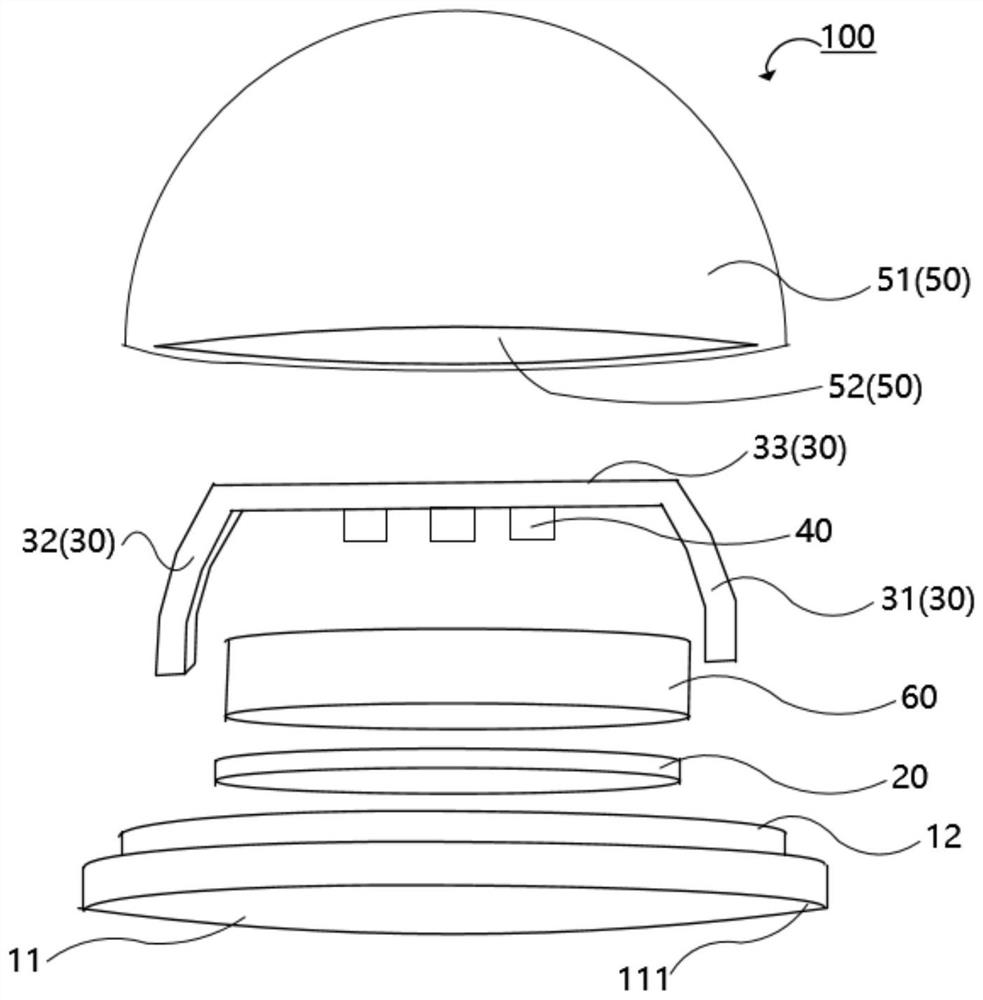
[0043] see figure 2 and image 3 , figure 2 A schematic diagram of a second three-dimensional structure of an LED packaging structure 100 provided in an embodiment of the present application; image 3This is an exploded view or an exploded schematic view of a second three-dimensional structure of an LED package structure 100 provided in an embodiment of the present application. figure 2 and figure 1 The difference is figure 2 The middle LED package structure further includes a lens 50 .
[0044] In some embodiments, the LED package structure 100 further includes a lens 50 , the lens 50 is disposed on a side of the bracket 30 away from the groove 13 , and the lens 50 is connected to the side wall 12 .
[0045] Specifically, the lens 50 is arranged on the side of the bracket 30 away from t...
Embodiment 3
[0059] This embodiment is the same as or similar to the above-mentioned embodiment, and the difference lies in that the features of the LED package structure are further described.
[0060] In some embodiments, the bracket 30 includes an arc-shaped first end portion 31 and a second end portion 32, and a middle portion 33 connected between the first end portion 31 and the second end portion 32, and the middle portion 33 is Flat, the LED chip 40 is disposed on the middle portion 33 .
[0061] Specifically, in order to facilitate the arrangement of the LED chips, the middle portion 33 of the bracket 30 is set as a plane, and the LED chips are arranged on the surface of the middle portion 33 facing the quantum dot layer 20 .
[0062] Specifically, the first end portion 31 and the second end portion 32 are both arc-shaped, which can facilitate setting the bracket 30 on the housing 10 and make the LED chip and the quantum dot layer 20 farther away.
[0063] In some embodiments, the...
PUM
 Abstract
Description
Claims
Application Information


