Simulation method and simulation device for quantum effect semiconductor, and storage medium

A technology of quantum effects and simulation methods, applied in the field of semiconductor simulation, can solve the problems of unstable calculation array, difficult model, non-convergence of iterative algorithm, etc., to achieve excellent convergence, ensure accuracy, and improve simulation accuracy.

Pending Publication Date: 2022-07-08
ACAD OF MATHEMATICS & SYSTEMS SCIENCE - CHINESE ACAD OF SCI
View PDF0 Cites 0 Cited by
  • Summary
  • Abstract
  • Description
  • Claims
  • Application Information

AI Technical Summary

Problems solved by technology

[0004] However, in the actual application process, the strong coupling and nonlinearity of the QDD model have brought great difficulties to the numerical solution of the model. The instability of the calculation array and the non-convergence of the iterative algorithm have caused great troubles for technicians in the actual simulation and calculation process

Method used


Image

  • Simulation method and simulation device for quantum effect semiconductor, and storage medium
  • Simulation method and simulation device for quantum effect semiconductor, and storage medium
  • Simulation method and simulation device for quantum effect semiconductor, and storage medium

Examples


Embodiment Construction

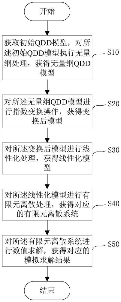
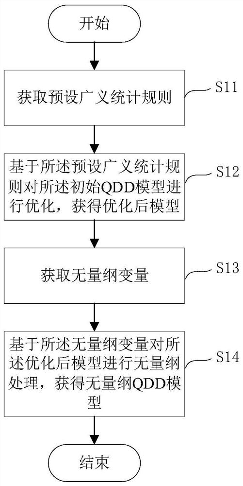
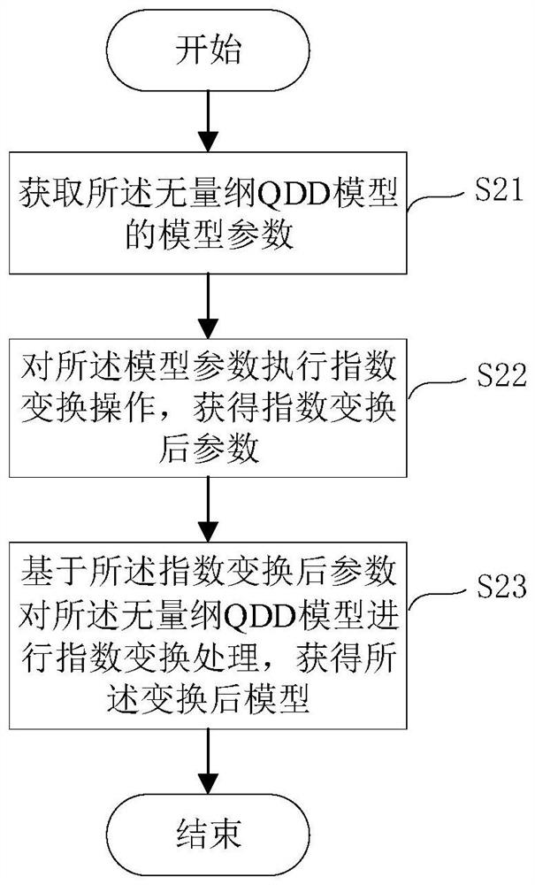
[0039] The specific implementations of the embodiments of the present invention will be described in detail below with reference to the accompanying drawings. It should be understood that, the specific embodiments described herein are only used to illustrate and explain the embodiments of the present invention, and are not used to limit the embodiments of the present invention.

[0040] The terms "system" and "network" in the embodiments of the present invention may be used interchangeably. "Plurality" refers to two or more than two, and in view of this, in the embodiment of the present invention, "plurality" can also be understood as "at least two". "And / or", which describes the association relationship of the associated objects, means that there can be three kinds of relationships, for example, A and / or B, which can mean that A exists alone, A and B exist at the same time, and B exists alone. In addition, the character " / ", unless otherwise specified, generally indicates th...


PUM


Abstract

The invention discloses a simulation method and device for a quantum effect semiconductor and a storage medium, and the method comprises the steps: obtaining an initial QDD model, and carrying out the dimensionless processing of the initial QDD model, and obtaining a dimensionless QDD model; performing exponential transformation operation on the dimensionless QDD model to obtain a transformed model; performing linearization processing on the transformed model to obtain a linearized model; performing finite element discrete processing on the linearized model to obtain a corresponding finite element discrete system; and carrying out numerical solution on the finite element discrete system to obtain a corresponding simulation solution result. According to the method, an original QDD model is optimized, and the finite element discrete system capable of accurately representing the characteristics of the semiconductor with the quantum effect is obtained in a mode of combining exponential processing, linear processing and discretization processing, so that the simulation accuracy is improved, and the actual simulation requirement is met.

Description

technical field [0001] The present invention relates to the technical field of semiconductor simulation, in particular to a simulation method for quantum effect semiconductors, a simulation device for quantum effect semiconductors, and a computer-readable storage medium. Background technique [0002] With the continuous development of semiconductor technology, the manufacturing size of semiconductor devices is getting smaller and smaller, so the requirements for semiconductor manufacturing are also getting higher and higher. Because semiconductor device fabrication is time-consuming and expensive, accurately designing and simulating nanoscale semiconductor devices plays an important role in the field of semiconductor fabrication. [0003] As modern semiconductor devices move towards the nanoscale, quantum mechanical phenomena are becoming more prominent and must be considered in numerical simulations. Since the classical drift-diffusion (DD) model is insufficient to describ...

Claims


Application Information

Patent Timeline
IPC IPC(8): G06F30/23G06F111/10
CPCG06F30/23G06F2111/10Y02E60/00
Inventor 崔涛郑伟英穆朋聪
Owner ACAD OF MATHEMATICS & SYSTEMS SCIENCE - CHINESE ACAD OF SCI
Why Eureka
Try Eureka