Light emitting diode and light emitting device thereof

A technology of light-emitting diodes and semiconductors, which is applied to electrical components, circuits, semiconductor devices, etc., can solve the problems of difficult process window manufacturing, smaller light-emitting area, and reduced brightness, and achieves the effect of expanding the process window.

Pending Publication Date: 2022-07-08
XIAMEN SANAN OPTOELECTRONICS CO LTD
View PDF0 Cites 0 Cited by
  • Summary
  • Abstract
  • Description
  • Claims
  • Application Information

AI Technical Summary

Problems solved by technology

[0002] The current vertical product technology only uses N-type conductive holes in the light-emitting area to achieve the functions of current expansion and current reduction. The disadvantage is that after the area of ​​the N-hole increases, the light-emitting area (roughened surface) will also become smaller, reducing its brightness.
When the core particle size is getting smaller and smaller to make N-type conductive holes, the process window is limited due to the process platform, which causes difficulties in the process.

Method used


Image

  • Light emitting diode and light emitting device thereof
  • Light emitting diode and light emitting device thereof
  • Light emitting diode and light emitting device thereof

Examples


Embodiment Construction

[0062] The embodiments of the present application are described below through specific specific examples, and those skilled in the art can easily understand other advantages and effects of the present application from the contents disclosed in this specification. The present application can also be implemented or operated through other different specific embodiments, and various details in the present application can also be modified or changed based on different viewpoints and applications without departing from the spirit of the present application.

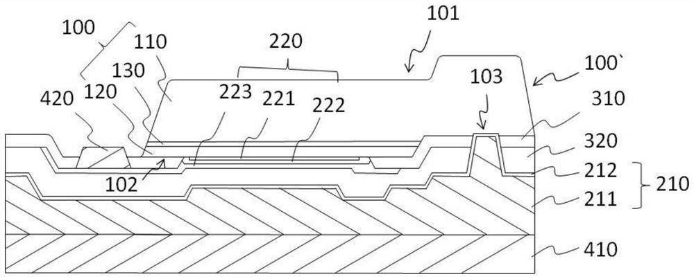
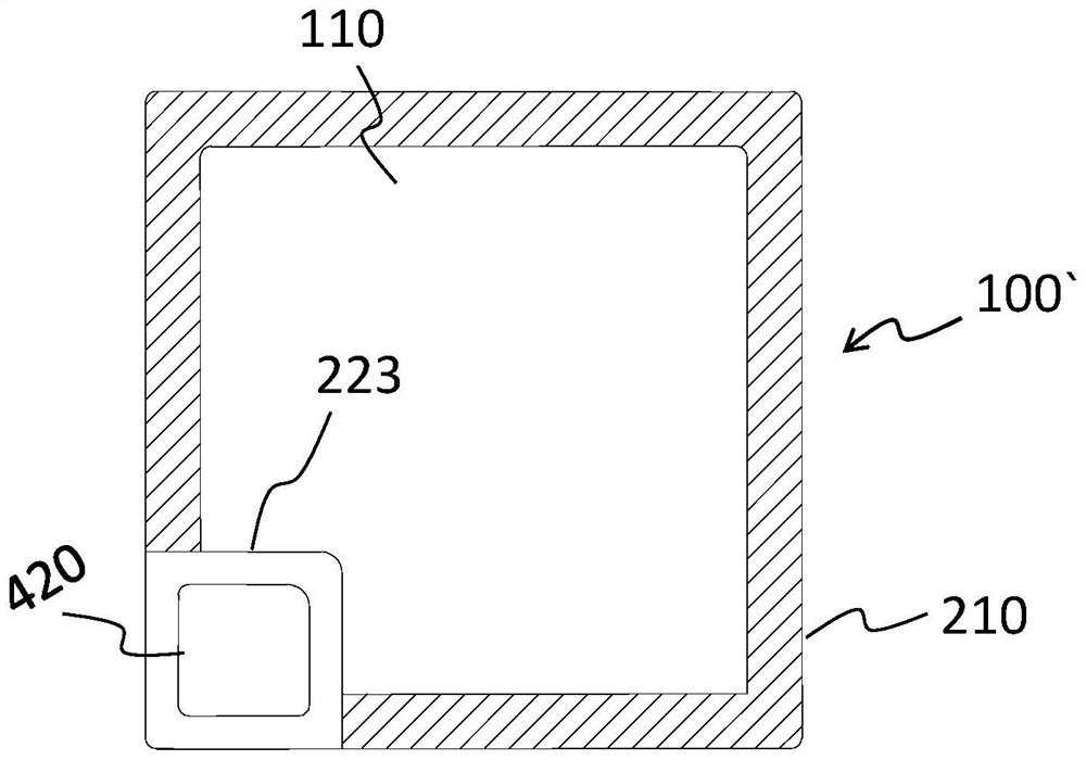
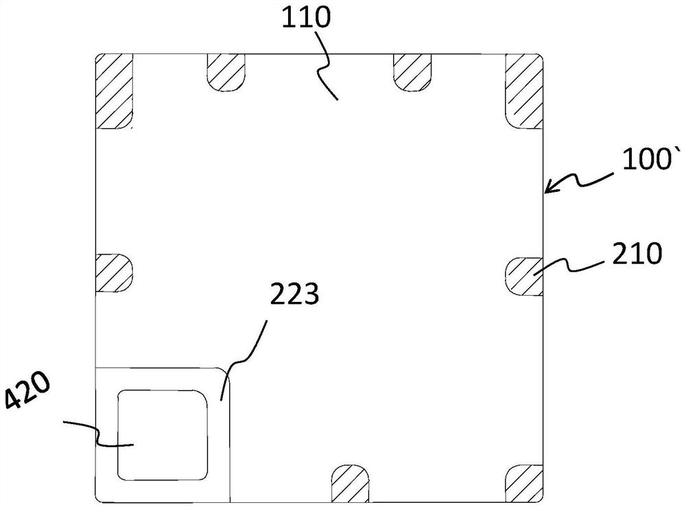
[0063] see Figure 1 to Figure 3 , in the first embodiment of the present invention, a light-emitting diode is disclosed, comprising: a semiconductor layer sequence 100 as an epitaxial structure, the semiconductor layer sequence 100 has sidewalls 100' and a first surface 101 and a second surface 101 oppositely disposed A surface 102 comprising a first-type semiconductor layer 110, a second-type semiconductor layer 120 arranged ...


PUM

PropertyMeasurementUnit
particle sizeaaaaaaaaaa
angleaaaaaaaaaa
particle sizeaaaaaaaaaa

Abstract

The invention discloses a light-emitting diode, which comprises a semiconductor layer sequence which is provided with a side wall and a first surface and a second surface which are oppositely arranged, and comprises semiconductor layer sequences which are sequentially arranged between the first surface and the second surface, the second surface is provided with a recess which at least penetrates through the active layer, the second type semiconductor layer and part of the first type semiconductor layer, the first electric connection layer is electrically connected with the first type semiconductor layer through the recess, and the first electric connection layer comprises reflective metal; the concave part is located on the side wall, and at least the side wall above the concave part is provided with surface roughening, thereby preventing chip technology yellow light processing abnormity caused by reflection metal, and improving product yield.

Description

technical field [0001] The present invention relates to a photoelectric element, in particular to a light-emitting diode structure and a light-emitting device thereof. Background technique [0002] The current vertical product process only uses the N-type conductive holes in the light-emitting area to achieve the functions of current expansion and current reduction. . When the size of the core particle is getting smaller and smaller, the N-type conductive hole is made, and the process window is limited due to the limitation of the process platform, which causes difficulties in the process. SUMMARY OF THE INVENTION [0003] In order to solve the technical problems in the background art, a light-emitting diode is proposed, including: [0004] Semiconductor layer sequence with sidewalls and first and second surfaces disposed oppositely, including semiconductor layers of a first type arranged in sequence between said first and second surfaces, an active layer designed to gen...

Claims


Application Information

Patent Timeline
Patent Type & Authority Applications(China)
IPC IPC(8): H01L33/22H01L33/46
CPCH01L33/22H01L33/46
Inventor 张博扬林凡威林信泰张中英
Owner XIAMEN SANAN OPTOELECTRONICS CO LTD
Why Eureka
Try Eureka