Charge pump circuit and nonvolatile memory

A charge pump and circuit technology, applied in static memory, instruments, and conversion equipment without intermediate conversion to AC, etc., can solve the problems that the transmission transistor cannot be fully turned on and reduce the ability to transmit current, so as to improve the current transmission capacity. Effect of reducing charge loss

Pending Publication Date: 2022-07-19
GIGADEVICE SEMICON (BEIJING) INC
View PDF0 Cites 0 Cited by
  • Summary
  • Abstract
  • Description
  • Claims
  • Application Information

AI Technical Summary

Problems solved by technology

At present, the transfer transistor in the boost stage unit of the charge pump circuit is not fully turned on, which reduces the ability to transfer current. Therefore, a charge pump circuit with higher current transfer capability is required

Method used


Image

  • Charge pump circuit and nonvolatile memory
  • Charge pump circuit and nonvolatile memory
  • Charge pump circuit and nonvolatile memory

Examples


Embodiment Construction

[0023] Various embodiments of the present invention will be described in more detail below with reference to the accompanying drawings. In the various figures, the same elements are designated by the same or similar reference numerals. For the sake of clarity, various parts in the figures have not been drawn to scale.

[0024] The charge pump circuit provided in this application is described by taking the application in a non-volatile memory as an example.

[0025] The specific embodiments of the present invention will be described in further detail below with reference to the accompanying drawings and embodiments.

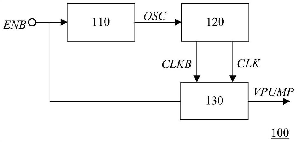
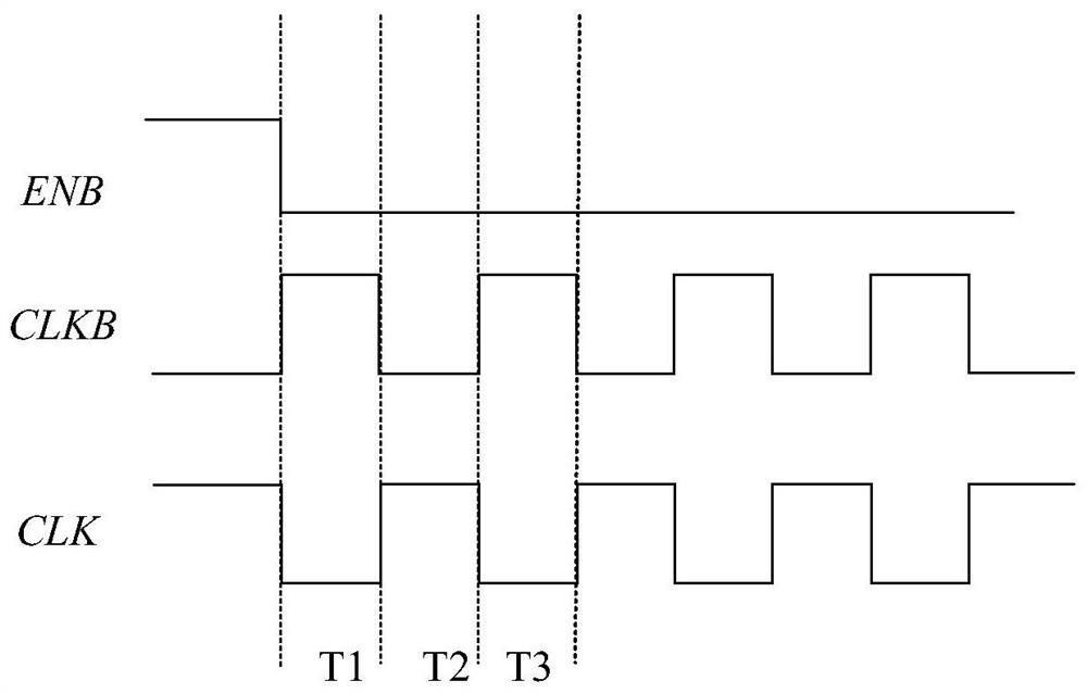
[0026] figure 1 A schematic structural diagram of a high-voltage generating unit in a non-volatile memory according to an embodiment of the present invention is shown, figure 2 A timing diagram of input signals in a charge pump circuit according to an embodiment of the present invention is shown.

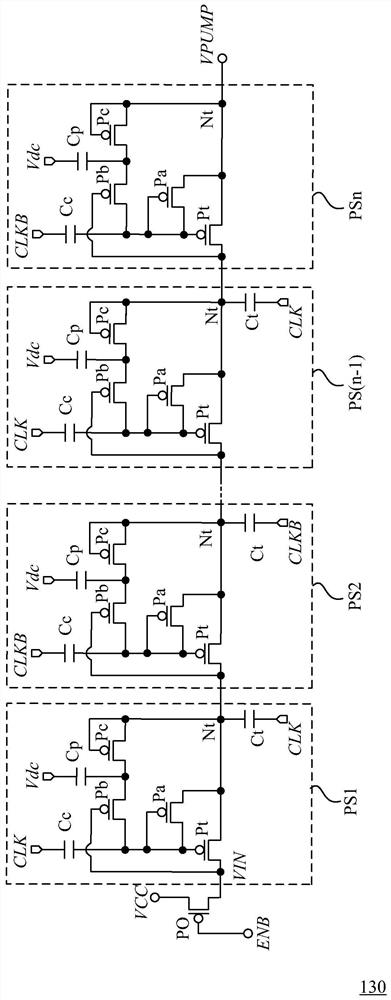
[0027] like figure 1 As shown, the high voltage generating u...


PUM


Abstract

The invention discloses a charge pump circuit and a nonvolatile memory. The charge pump circuit comprises a plurality of boost-stage charge pump units which are connected in series, and each boost-stage charge pump unit comprises an input end; an output terminal; a first capacitor; the first end of the second capacitor is connected with the output end; a third capacitor; the control end of the first switch tube is connected with the first end of the first capacitor, the first access end is connected with the input end, and the second access end is connected with the output end; a first one-way conduction element; the control end of the third switch tube is connected with the input end, the first access end is connected with the first end of the first capacitor, and the second access end is connected with the first end of the third capacitor; in the charge storage stage, the first switch tube is switched on, and the second capacitor is charged; in the charge release stage, the second capacitor provides charges for the next-stage charge pump, and the charges at the control end of the first switching tube are transferred to the third capacitor through the third switching tube. The first switch tube in the charge pump unit can be fully conducted, and the current transmission capability of the charge pump circuit is improved.

Description

technical field [0001] The present invention relates to the technical field of integrated circuits, and more particularly, to a charge pump circuit and a nonvolatile memory. Background technique [0002] When NVM (Non-Volatile Memory) works, several high voltages are generated on-chip through low-voltage power supplies for reading, erasing and writing operations of memory cells. These voltages are usually set by the internal charge. The Charge Pump circuit is generated. A charge pump circuit, also known as a switched capacitor voltage converter, is a DC-DC (converter) that utilizes "flying" or "pumping" capacitors (rather than inductors or transformers) to store energy. [0003] The charge pump circuit receives the low voltage power supply and boosts the voltage through multiple stages, and then the output stage of the charge pump circuit outputs the target high voltage. Currently, the transfer transistor in the boost stage unit of the charge pump circuit cannot be fully t...

Claims


Application Information

Patent Timeline
Patent Type & Authority Applications(China)
IPC IPC(8): H02M3/07G11C5/14
CPCH02M3/07G11C5/145
Inventor 张现聚刘铭邓龙利
Owner GIGADEVICE SEMICON (BEIJING) INC
Why Eureka
Try Eureka