Wafer storage library and transfer system

A wafer storage and storage technology, applied in storage devices, transportation and packaging, conveyor objects, etc., can solve the problems of low wafer access and transfer efficiency, and achieve the effect of ensuring transfer efficiency and access efficiency.

Pending Publication Date: 2022-07-22
MEETFUTURE TECH (SHANGHAI) CO LTD
View PDF10 Cites 2 Cited by
  • Summary
  • Abstract
  • Description
  • Claims
  • Application Information

AI Technical Summary

Problems solved by technology

[0003] In the semiconductor manufacturing process, it is often necessary to access the wafers in the storage library. Since the storage library is generally multi-layer storage, in the process of wafer access, it is often necessary to access the wafers of different layers. The storage and retrieval of wafers is carried out, and the transfer of wafers is carried out through traditional stackers, resulting in low wafer access and transfer efficiency

Method used


Image

  • Wafer storage library and transfer system
  • Wafer storage library and transfer system
  • Wafer storage library and transfer system

Examples


Embodiment Construction

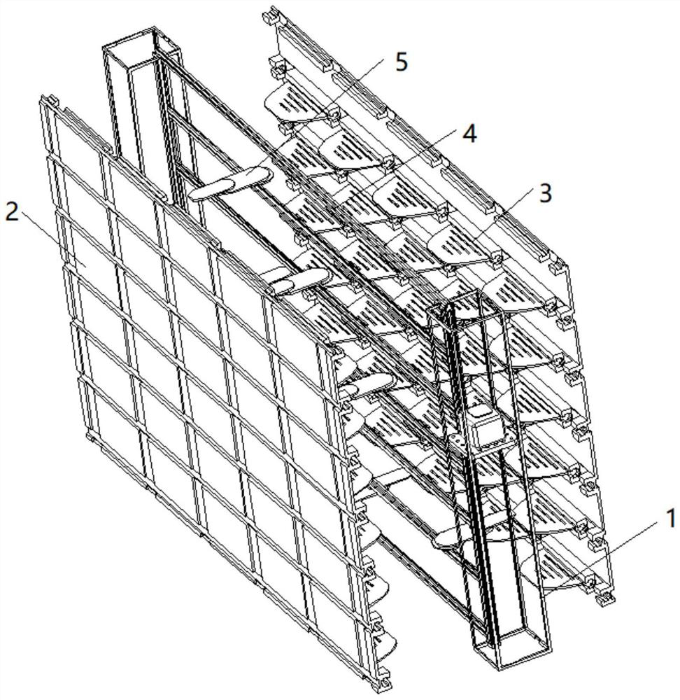
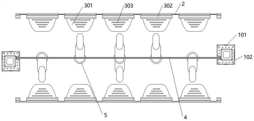
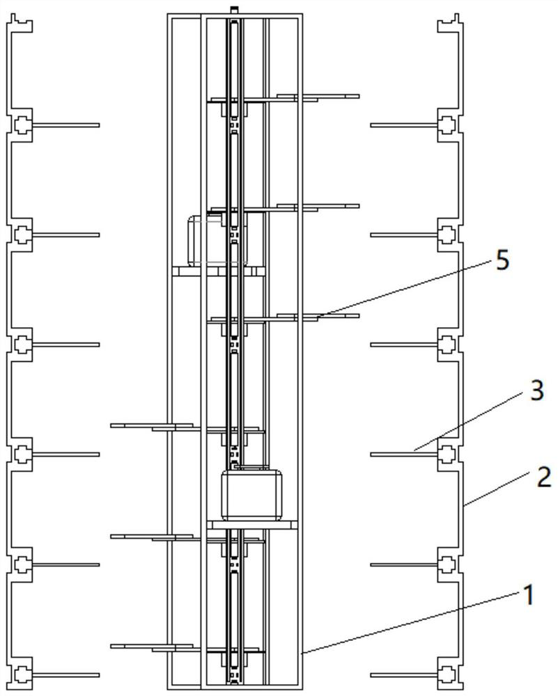
[0028] The embodiments of the present application will be described in detail below with reference to the accompanying drawings.

[0029] The embodiments of the present application are described below through specific specific examples, and those skilled in the art can easily understand other advantages and effects of the present application from the contents disclosed in this specification. Obviously, the described embodiments are only a part of the embodiments of the present application, but not all of the embodiments. The present application can also be implemented or applied through other different specific embodiments, and various details in this specification can also be modified or changed based on different viewpoints and applications without departing from the spirit of the present application. It should be noted that the following embodiments and features in the embodiments may be combined with each other under the condition of no conflict. Based on the embodiments ...


PUM


Abstract

The invention provides a wafer storage library and a transfer system. The storage library comprises two sets of lifting mechanisms; the rails are arranged between the two sets of lifting mechanisms, the rails are sequentially arranged from top to bottom, the two ends of each rail are connected with the two sets of lifting mechanisms respectively, and storing and taking mechanisms are arranged on the rails; the storage racks are arranged on the two sides of the rails, the two storage racks are each provided with a plurality of layers of storage stations, the storage stations are used for storing wafers, and the rails correspond to the storage stations in a one-to-one mode. The lifting mechanisms are arranged on the two sides of the storage frame to transfer the wafers, the transfer efficiency of the wafers is guaranteed, the rails corresponding to the multiple layers of storage stations one to one are arranged, and the storage and taking mechanisms used for storing and taking the wafers are arranged on the rails, so that the storage and taking efficiency of the wafers is guaranteed.

Description

technical field [0001] The present specification relates to the technical field of semiconductor wafer access, in particular to a wafer storage library and a transfer system. Background technique [0002] In the semiconductor industry, wafers are an important part of them. Wafers refer to silicon wafers used to make silicon semiconductor circuits. High-purity polysilicon is dissolved and mixed with silicon crystal seeds, and then slowly pulled out to form a cylindrical shape. of monocrystalline silicon. The silicon ingot is ground, polished and sliced ​​to form a silicon wafer, that is, a wafer. [0003] In the semiconductor manufacturing process, it is often necessary to access the wafers in the storage library. Since the storage library is generally multi-layer storage, in the process of accessing the wafers, it is often necessary to access the wafers of different layers. The access work is carried out in a circle, and the transfer of the wafers is carried out by the tra...

Claims


Application Information

Patent Timeline
Patent Type & Authority Applications(China)
IPC IPC(8): B65G1/04B65G1/137B65G47/90
CPCB65G1/04B65G1/1373B65G47/902
Inventor 缪峰
Owner MEETFUTURE TECH (SHANGHAI) CO LTD
Why Eureka
Try Eureka